
Digital Holographic Inspection Systems Market Size and Share
Market Overview
| Study Period | 2020 - 2031 |
|---|---|
| Market Size (2026) | USD 0.37 Billion |
| Market Size (2031) | USD 1.10 Billion |
| Growth Rate (2026 - 2031) | 24.35 % |
| Fastest Growing Market | Asia-Pacific |
| Largest Market | North America |
| Market Concentration | Medium |
Major Players *Disclaimer: Major Players sorted in no particular order Image © Mordor Intelligence. Reuse requires attribution under CC BY 4.0. | |
Digital Holographic Inspection Systems Market Analysis by Mordor Intelligence
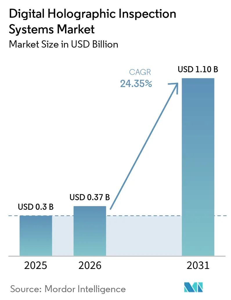
The Digital Holographic Inspection Systems Market size was valued at USD 0.30 billion in 2025 and estimated to expand from USD 0.37 billion in 2026 to USD 1.10 billion by 2031, at a CAGR of 24.35% during the forecast period (2026-2031). Advanced packaging is increasing the need for non-contact, three-dimensional inspection in semiconductor production. Holographic tools can measure surfaces and subsurface features without touching sensitive parts. Factory adoption also depends on systems that can operate within production lines rather than only in laboratories. Software-led reconstruction and defect classification are making these systems easier to use in repeatable workflows. High costs of equipment, integration, and skills still limit adoption outside high-value manufacturing applications.
Key Report Takeaways
- By the holographic technology segment, Digital Holographic Interferometry held 31.34% of the Digital Holographic Inspection Systems market share in 2025, while Computer-Generated Holography is projected to expand at a CAGR of 27.77% through 2031.
- By inspection type, Surface and Defect Inspection accounted for 29.51% of the Digital Holographic Inspection Systems market size in 2025, while Internal and Subsurface Inspection is projected to expand at a CAGR of 27.61% through 2031.
- According to the system configuration, Inline Inspection Systems held 41.29% of market revenue in 2025, while Portable and Handheld Inspection Systems are projected to expand at a CAGR of 29.91% through 2031.
- By end-user, Semiconductor Manufacturers held 25.51% of the Digital Holographic Inspection Systems Market revenue in 2025 and are projected to expand at a CAGR of 28.71% through 2031.
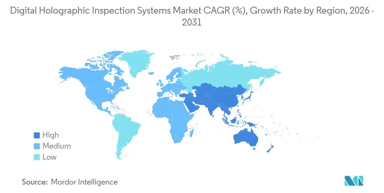
- By geography, North America held 32.34% of market revenue in 2025, while Asia-Pacific is projected to expand at a CAGR of 27.91% through 2031.
Note: Market size and forecast figures in this report are generated using Mordor Intelligence’s proprietary estimation framework, updated with the latest available data and insights as of January 2026.
Market Trends and Insights
Drivers Impact Analysis of Digital Holographic Inspection Systems Market*
| Driver | (~) % Impact on CAGR Forecast | Geographic Relevance | Impact Timeline |
|---|---|---|---|
| Advanced-Packaging Inspection Demand | +5.2% | Global, strongest in Asia-Pacific and North America | Short term (≤ 2 years) |
| Non-Contact Full-Field Measurement | +4.8% | Global, concentrated in Europe and North America | Medium term (2-4 years) |
| AI-Assisted Defect Classification and Reconstruction | +4.5% | Global, led by North America and Asia-Pacific | Medium term (2-4 years) |
| Inline Quality Control and Industry 4.0 Integration | +3.9% | Europe and North America, extending to Asia-Pacific industrial zones | Medium term (2-4 years) |
| Holographic Metrology With Atomic Force Microscopy | +2.7% | North America and Asia-Pacific, with early gains in Germany | Long term (≥ 4 years) |
| Label-Free Imaging for Cell and Gene Therapy Research | +2.1% | North America and Europe, with early adoption in Japan and South Korea | Long term (≥ 4 years) |
| Source: Mordor Intelligence | |||
Semiconductor Advanced-Packaging Inspection Demand
The Digital Holographic Inspection Systems Market is benefiting from heterogeneous integration and advanced packaging. These processes use 2.5D interposers, fan-out wafer-level packaging, and wafer-to-wafer hybrid bonding. Each architecture adds overlay, bonding, and void-detection requirements that conventional two-dimensional optical tools cannot always meet. Coherent-light phase imaging can identify refractive-index differences in transparent substrates. This supports inspection of subsurface voids and misaligned redistribution layers in co-packaged optics and through-glass-via platforms. Semiconductor Equipment and Materials International requirements can favor suppliers with established cleanroom-ready designs.
Non-Contact Full-Field Surface Measurement
Fraunhofer IPM states that its HoloTop sensor family evaluates more than 100 million measurement points per second. The sensor delivers sub-micrometer accuracy in less than 100 milliseconds for coin-sized objects.[1] Fraunhofer IPM also integrated this technology into production-line coordinate measuring machines. This reduces measurement time without physical contact. Its bipolar-plate sensor measures metal plates up to 400 mm x 150 mm in 1 pass. The Digital Holographic Inspection Systems Market can extend from standalone metrology into process-control software where full-field data supports digital-twin workflows.
AI-Assisted Defect Classification and Reconstruction
A 2026 Scientific Reports study introduced hardware-agnostic datasets to test the limits of AI detection in digital holographic microscopy.[2] The work addresses the challenge of transferring models between optical setups. Better portability can reduce the need to rebuild models for each instrument. A 2026 Measurement article also used polarization-sensitive dark-field digital holographic microscopy to classify randomly oriented wafer scratches. The Digital Holographic Inspection Systems Market is consequently moving toward competition based on software and sensor performance. Suppliers need data and software capabilities as algorithms shorten calibration and reduce routine operating complexity.[3]
Inline Quality Control and Industry 4.0 Integration Fraunhofer IPMS and DIVE reported in July 2025 that targeted inspectio
Fraunhofer IPMS and DIVE reported in July 2025 that targeted inspection could eliminate at least 25% of control wafers. The project also reported savings of more than 118,000 kilograms of CO2 each month in a 28 nm process with 25,000 wafer starts per month. A 2025 study described a phase-randomizing mirror that reduces coherent noise without mechanical modulation hardware.[4] Shorter exposures can improve deployment in vibration-prone settings. Industrial cybersecurity requirements can add qualification cost when sensors connect to manufacturing execution systems. Suppliers with open communication architectures may be better placed to support factory modernization.
Restraints Impact Analysis of Digital Holographic Inspection Systems Market*
| Restraint | (~) % Impact on CAGR Forecast | Geographic Relevance | Impact Timeline |
|---|---|---|---|
| High Instrument and Integration Costs | -2.8% | Global, most acute in South America, the Middle East and Africa, and smaller Southeast Asian markets | Short term (≤ 2 years) |
| Specialized Optical and Computational Expertise | -2.1% | Global, most severe outside North America and Western Europe | Medium term (2-4 years) |
| Coherence Noise, Vibration, and Contamination Sensitivity | -1.5% | Global, strongest in high-throughput Asia-Pacific plants | Medium term (2-4 years) |
| Limited MES and SPC Interoperability | -1.2% | North America and Europe, where legacy systems are common | Long term (≥ 4 years) |
| Source: Mordor Intelligence | |||
High Instrument and Integration Costs
A production-grade system can cost more than USD 200,000. The cost can approach USD 1 million when custom optics, vibration isolation, cleanroom qualification, and software integration are included. This narrows adoption among mid-sized manufacturers and emerging packaging facilities. Connecting sensors to manufacturing execution system layers, defect databases, and statistical process control dashboards also requires engineering work. Modular designs and OPC Unified Architecture connectivity can reduce some of the burden. Legacy proprietary platforms continue to slow the deployment of fixed inline systems.
Requirement for Specialized Optical and Computational Expertise
Accurate operation requires coherent-optics alignment, wavefront reconstruction, phase-unwrapping procedures, and AI model validation. Small alignment or thermal changes can create systematic measurement errors that affect process-control decisions. A 2025 study found that a single calibration step could support monitoring within a known polymer. Establishing that calibration still requires specialist knowledge. Automated calibration, recipe-based interfaces, and remote support can reduce the burden for operators. The skills gap remains significant outside specialist metrology teams and research centers.
*Our forecasts treat driver/restraint impacts as directional, not additive. The impact forecasts reflect baseline growth, mix effects, and variable interactions.
Digital Holographic Inspection Systems Market Segment Analysis
By Holographic Technology:
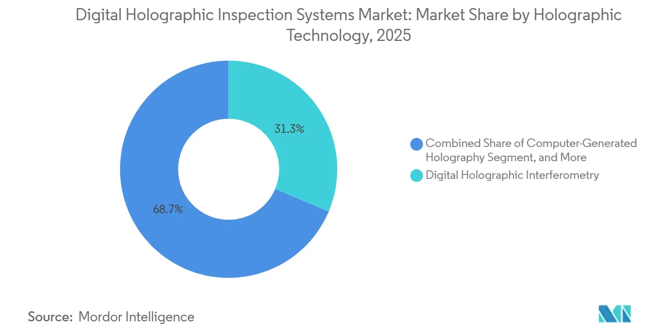
Interferometry Holds a Strong Installed Base While CGH AdvancesDigital Holographic Interferometry accounted for 31.34% of market revenue in 2025. It is established in deformation measurement, aerospace non-destructive testing, and semiconductor overlay metrology. Its phase sensitivity supports displacement measurements below 1 nm. A 2026 SAE paper used holographic vibration analysis to detect kissing-bond defects by tracking changes in natural frequency.
Computer-Generated Holography is projected to expand at a CAGR of 27.77% through 2031. It supplies reference wavefronts for asphere testing in EUV and high-numerical-aperture EUV lithography. Holographic Phase Imaging serves transparent-substrate defect analysis, while Fourier and Fresnel digital holography reconstruct complex wavefronts in photonics testing. The Digital Holographic Inspection Systems industry benefits from both the mature demand for interferometry and the use of CGH in lithography qualification.

By Inspection Type:
Surface Inspection Leads While Subsurface Use ExpandsSurface and Defect Inspection held 29.51% of market revenue in 2025. The segment identifies particles, discoloration, scratches, and geometric nonconformities on micro-components and wafer surfaces. Fraunhofer IPM reports that HoloAMS systems provide two-dimensional and three-dimensional topography across areas up to 400 mm x 150 mm. Dimensional, deformation, thickness, and profile inspection serve factory automation, structural monitoring, thin films, and transparent substrates.
Internal and Subsurface Inspection is projected to expand at a CAGR of 27.61% through 2031. The Digital Holographic Inspection Systems market size for this type benefits from demand for through-glass vias, embedded chiplets, and co-packaged optical devices. These features cannot be fully assessed by surface-only metrology. Refractive-index sensitivity of 10^-4 can support visualization of internal defects in glass-core interposers and related materials.
By System Configuration:
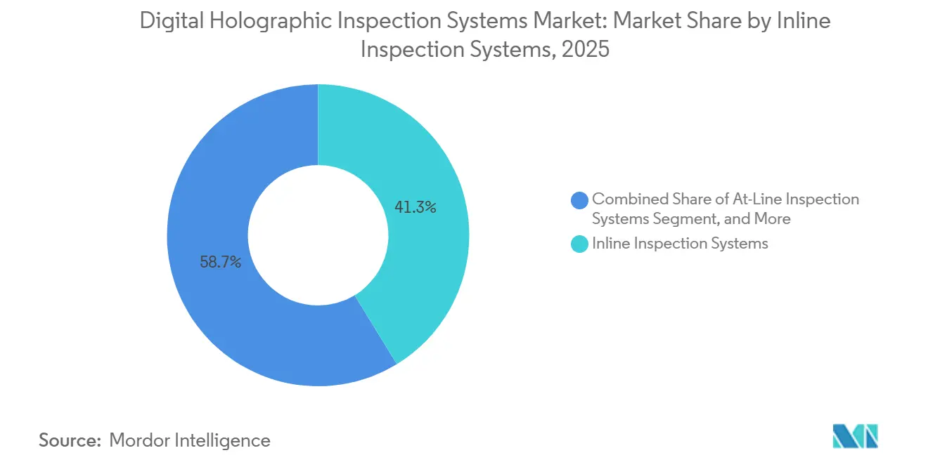
Inline Systems Lead While Handheld Platforms Add FlexibilityInline Inspection Systems accounted for 41.29% of market revenue in 2025. Continuous inspection can prevent defects from moving to downstream assembly. Fraunhofer IPM states that its integrated holographic sensor can provide sub-micrometer accuracy without contact. At-Line and Offline Laboratory systems remain suitable for sampling, research, and tool qualification.
Portable and Handheld Inspection Systems are projected to expand at a CAGR of 29.91% through 2031. They support aerospace maintenance work and the inspection of modules that cannot be moved. Smaller coherent laser sources, compact CMOS sensors, and GPU-accelerated reconstruction enable this shift. The 2025 multiwavelength holography research demonstrated coherence control in vibration-prone settings.
By End-User:
Semiconductor Manufacturers Combine Scale and Fast ExpansionSemiconductor Manufacturers held 25.51% market share in the Digital Holographic Inspection Systems market in 2025. They are projected to expand at a CAGR of 28.71% through 2031. Heterogeneous integration creates overlay, bonding-quality, and subsurface-void requirements at each interface in a three-dimensional stack. Electronics and Advanced-Packaging Manufacturers have similar needs across glass, organic laminate, and silicon interposers.
Automotive manufacturers use holographic systems for powertrain deformation and fuel-cell bipolar-plate inspection. Aerospace and defense organizations use the technology for composite panel and adhesive bond evaluation. Optical and photonics manufacturers use it to test lenses, aspheres, and diffractive optical elements. Semiconductor requirements remain influential because they set high standards for integration and repeatability.
Geography Analysis
North America Digital Holographic Inspection Systems Market
North America held 32.34% of market revenue in 2025. The United States is home to semiconductor fabs, defense contractors, and aerospace maintenance facilities. CHIPS and Science Act funding is supporting domestic manufacturing and investment in advanced packaging. Canada and Mexico add demand through automotive supply chains. The Digital Holographic Inspection Systems Market has a broad commercial base in the region.
Europe Digital Holographic Inspection Systems Market
Europe held the second-largest geographic position in 2025. Germany is central through automotive, tooling, and electronics production. Fraunhofer IPM is commercializing the HoloAMS inline system and HoloTop sensor family for production measurement. The United Kingdom, France, Italy, and Spain contribute through precision optics, aerospace testing, and regulated bioprocessing. Machinery rules can encourage the replacement of legacy inspection equipment.
APAC, MEA and South America Digital Holographic Inspection Systems Market
Asia-Pacific is projected to expand at a CAGR of 27.91% through 2031. Taiwan, South Korea, Japan, and China anchor semiconductor packaging activity. Hamamatsu Photonics launched a system that measures the full surface of 300 mm wafers in 5 seconds. Takano markets the DHI-2000 for simultaneous surface, back-surface, and internal-defect detection, while India is building semiconductor capacity, and the Middle East, Africa, and South America offer an entry route for portable systems.
Competitive Landscape
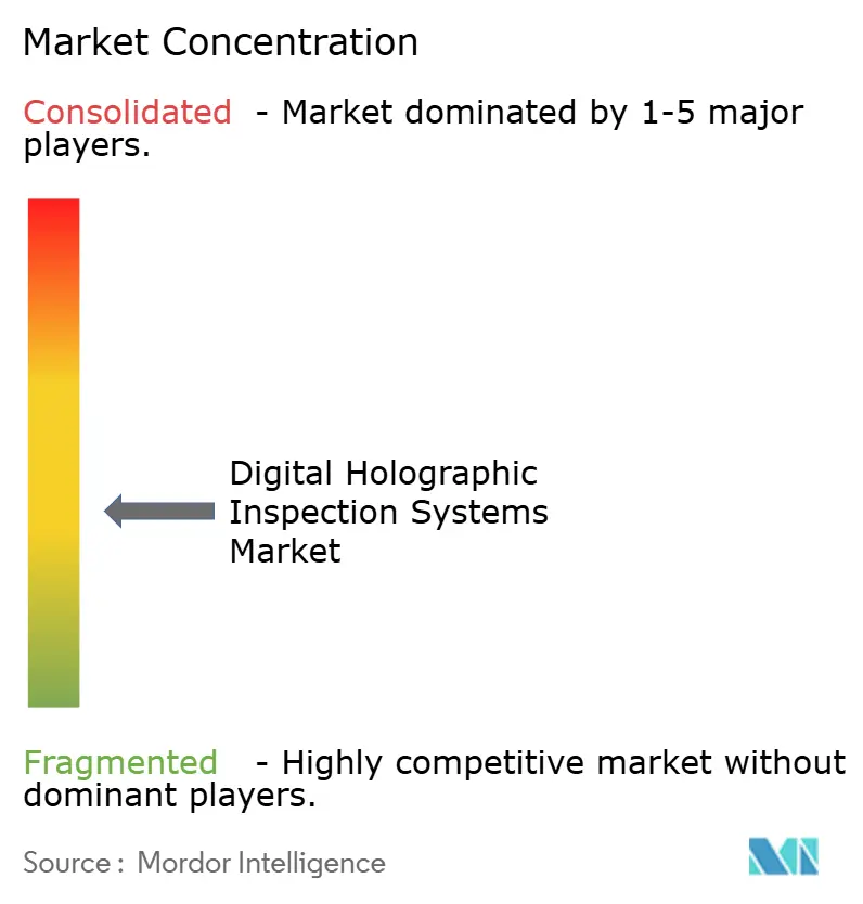
The Digital Holographic Inspection Systems Market is moderately fragmented. Precision-metrology suppliers hold strong positions in semiconductor and industrial applications. Smaller specialists compete through focused sensors and reconstruction software. Competition centers on throughput, sensor size, software capability, and factory integration. Park Systems acquired Lyncée Tec in January 2025 to strengthen its optical metrology portfolio.
In June 2026, Park Systems and imec started a joint development program covering atomic force microscopy, digital holographic microscopy, white-light interferometry, and imaging spectroscopic ellipsometry. ZYGO presented its Nexview NX2 optical profiler, Qualifire laser interferometer, and CGH-capable Flatness and Asphere Tester at Optatec 2026. Phase Holographic Imaging launched an AI-enabled HoloMonitor in December 2025. These moves combine hardware, software, and application expertise. Rugged handheld equipment for aerospace maintenance remains open to specialist suppliers.
AI-enabled reconstruction can reduce operating complexity for mid-sized manufacturers. Suppliers also need data communication protocols that work with manufacturing execution systems and real-time statistical process control. Vendors without OPC Unified Architecture or SECS/GEM support may be excluded from some automation projects. Established suppliers retain an advantage through depth of research and application experience.
Digital Holographic Inspection Systems Industry Leaders
-
Park Systems Corp.
-
ZYGO Corporation
-
Carl Zeiss AG
-
Phase Holographic Imaging PHI AB
-
MetroLaser, Inc.
- *Disclaimer: Major Players sorted in no particular order
Digital Holographic Inspection Systems Market Companies Covered in this Report
- Park Systems Corp.
- ZYGO Corporation
- Carl Zeiss AG
- Phase Holographic Imaging PHI AB
- Holmarc Opto-Mechatronics Limited
- MetroLaser, Inc.
- RealView Imaging Ltd.
- Lyncee Tec SA
- Ovizio Imaging Systems NV
- Nanolive SA
- Holoeye Photonics AG
- Geola Digital UAB
- HoloTech Switzerland AG
- Holoxica Limited
- Optics11 B.V.
- Thorlabs, Inc.
- Hamamatsu Photonics K.K.
- Coherent Corp.
- MKS Instruments, Inc.
- Carl Zeiss SMT GmbH
Recent Industry Developments in Digital Holographic Inspection Systems Market
- September 2026: TSMC unveiled a materials and equipment supplier campus inside Kaohsiung's Baipu Industrial Park to accelerate qualification of next-generation inspection and bonding-process tools. The facility is projected to improve advanced-packaging validation efficiency by 25-50%.
- June 2026: Park Systems announced a multi-technology joint development program with imec integrating atomic force microscopy, digital holographic microscopy, imaging spectroscopic ellipsometry, and white-light interferometry into a unified metrology solution for advanced 3D packaging and logic research.
- May 2026: ZYGO presented its Nexview NX2 3D optical profiler, Qualifire 1.2 laser interferometer, and CGH-capable Flatness/Asphere Tester at Optatec 2026 in Frankfurt, Germany, targeting precision optical manufacturing and inspection across semiconductor, photonics, and industrial markets.
- March 2026: ZYGO launched the Qualifire laser interferometer line, incorporating an enhanced Flying Spot Module, stabilized lasers, stable zoom optics, and Smart Accessories that automatically configure lateral resolution and apply factory-calibrated system-error correction.
Global Digital Holographic Inspection Systems Market Report Scope
Digital Holographic Inspection Systems utilize advanced wavefront recording and reconstruction techniques to capture high-resolution 3D data of objects, enabling non-contact, high-precision measurement of surface topography, internal structures, and dynamic deformations for quality control in high-tech manufacturing and scientific research.
The Digital Holographic Inspection Systems Market Report is Segmented by Holographic Technology (Digital Holographic Interferometry, Digital Holographic Microscopy, Holographic Phase Imaging, Fourier and Fresnel Digital Holography, Computer-Generated Holography, and Other Holographic Technologies), Inspection Type (Surface and Defect Inspection, Dimensional and Geometric Inspection, Deformation and Displacement Measurement, Thickness and Profile Measurement, Internal and Subsurface Inspection, and Other Inspection Types), System Configuration (Inline Inspection Systems, At-Line Inspection Systems, Offline and Laboratory Inspection Systems, and Portable and Handheld Inspection Systems), End-User (Semiconductor Manufacturers, Electronics and Advanced-Packaging Manufacturers, Automotive Manufacturers and Suppliers, Aerospace and Defense Organizations, Optical and Photonics Manufacturers, Industrial Machinery and Precision Engineering Companies, and Other End-Users), and Geography (North America, South America, Europe, Asia-Pacific, Middle East and Africa). The Market Forecasts are Provided in Terms of Value (USD).
Segmentation Overview
| Digital Holographic Interferometry |
| Digital Holographic Microscopy |
| Holographic Phase Imaging |
| Fourier and Fresnel Digital Holography |
| Computer-Generated Holography |
| Other Holographic Technologies |
| Surface and Defect Inspection |
| Dimensional and Geometric Inspection |
| Deformation and Displacement Measurement |
| Thickness and Profile Measurement |
| Internal and Subsurface Inspection |
| Other Inspection Types |
| Inline Inspection Systems |
| At-Line Inspection Systems |
| Offline and Laboratory Inspection Systems |
| Portable and Handheld Inspection Systems |
| Semiconductor Manufacturers |
| Electronics and Advanced-Packaging Manufacturers |
| Automotive Manufacturers and Suppliers |
| Aerospace and Defense Organizations |
| Optical and Photonics Manufacturers |
| Industrial Machinery and Precision Engineering Companies |
| Other End-Users |
| North America | United States | |
| Canada | ||
| Mexico | ||
| South America | Brazil | |
| Argentina | ||
| Rest of South America | ||
| Europe | Germany | |
| United Kingdom | ||
| France | ||
| Italy | ||
| Spain | ||
| Rest of Europe | ||
| Asia-Pacific | China | |
| Japan | ||
| India | ||
| South Korea | ||
| Rest of Asia-Pacific | ||
| Middle East and Africa | Middle East | Saudi Arabia |
| Turkey | ||
| United Arab Emirates | ||
| Rest of the Middle East | ||
| Africa | South Africa | |
| Kenya | ||
| Rest of Africa | ||
| By Holographic Technology | Digital Holographic Interferometry | ||
| Digital Holographic Microscopy | |||
| Holographic Phase Imaging | |||
| Fourier and Fresnel Digital Holography | |||
| Computer-Generated Holography | |||
| Other Holographic Technologies | |||
| By Inspection Type | Surface and Defect Inspection | ||
| Dimensional and Geometric Inspection | |||
| Deformation and Displacement Measurement | |||
| Thickness and Profile Measurement | |||
| Internal and Subsurface Inspection | |||
| Other Inspection Types | |||
| By System Configuration | Inline Inspection Systems | ||
| At-Line Inspection Systems | |||
| Offline and Laboratory Inspection Systems | |||
| Portable and Handheld Inspection Systems | |||
| By End-User | Semiconductor Manufacturers | ||
| Electronics and Advanced-Packaging Manufacturers | |||
| Automotive Manufacturers and Suppliers | |||
| Aerospace and Defense Organizations | |||
| Optical and Photonics Manufacturers | |||
| Industrial Machinery and Precision Engineering Companies | |||
| Other End-Users | |||
| By Geography | North America | United States | |
| Canada | |||
| Mexico | |||
| South America | Brazil | ||
| Argentina | |||
| Rest of South America | |||
| Europe | Germany | ||
| United Kingdom | |||
| France | |||
| Italy | |||
| Spain | |||
| Rest of Europe | |||
| Asia-Pacific | China | ||
| Japan | |||
| India | |||
| South Korea | |||
| Rest of Asia-Pacific | |||
| Middle East and Africa | Middle East | Saudi Arabia | |
| Turkey | |||
| United Arab Emirates | |||
| Rest of the Middle East | |||
| Africa | South Africa | ||
| Kenya | |||
| Rest of Africa | |||
Key Questions Answered in the Report
What is the Digital Holographic Inspection Systems Market size?
The Digital Holographic Inspection Systems Market size is estimated at USD 0.37 billion in 2026 and is forecast to reach USD 1.10 billion by 2031.
What is driving demand for digital holographic inspection systems?
Advanced semiconductor packaging, non-contact full-field measurement, AI-assisted reconstruction, and inline quality control are key demand factors.
Which holographic technology has the largest revenue share?
Digital Holographic Interferometry held 31.34% of revenue in 2025, supported by industrial and semiconductor uses.
Which system configuration is expanding fastest?
Portable and Handheld Inspection Systems are projected to expand at a CAGR of 29.91% through 2031.
Which region is projected to expand fastest?
Asia-Pacific is projected to expand at a CAGR of 27.91% through 2031, supported by semiconductor packaging activity.
What limits wider adoption of holographic inspection systems?
High equipment and integration costs, specialized skills needs, and production-environment sensitivity limit adoption in some applications.