Consumer Electronics Semiconductor Silicon Wafer Market Size and Share
Market Overview
| Study Period | 2021 - 2031 |
|---|---|
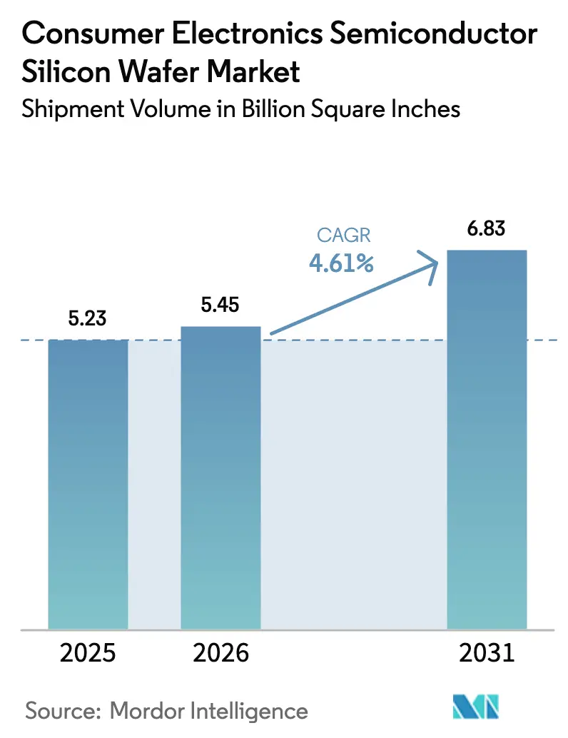
| Market Volume (2026) | 5.45 Billion Square Inches |
| Market Volume (2031) | 6.83 Billion Square Inches |
| Growth Rate (2026 - 2031) | 4.61% CAGR |
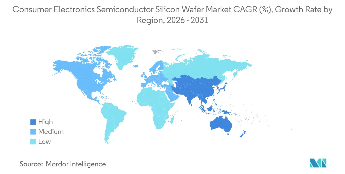
| Fastest Growing Market | Asia Pacific |
| Largest Market | Asia Pacific |
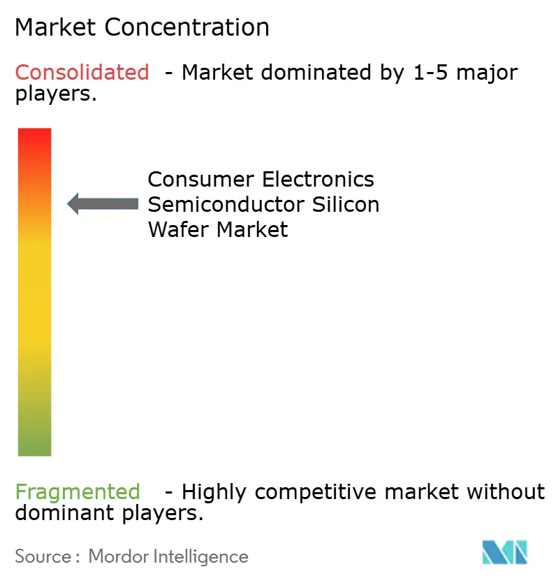
| Market Concentration | High |
Major Players *Disclaimer: Major Players sorted in no particular order Image © Mordor Intelligence. Reuse requires attribution under CC BY 4.0. | |
Consumer Electronics Semiconductor Silicon Wafer Market Analysis by Mordor Intelligence
The Consumer Electronics Semiconductor Silicon Wafer Market size in terms of shipment volume is projected to expand from 5.23 Billion Square Inches in 2025 and 5.45 Billion Square Inches in 2026 to 6.83 Billion Square Inches by 2031, registering a CAGR of 4.61% between 2026 to 2031. Strengthening demand for logic-intensive devices, migration to advanced node geometries, and government-backed fab incentives anchor this growth. Capital outlays by leading foundries continue to favor 300 mm substrates that maximize die counts, while specialty wafers such as silicon-on-insulator (SOI) gain share because they enable higher radio-frequency efficiency in 5G smartphones. Conversely, trailing-edge 200 mm capacity faces enduring margin pressure as analog and discrete devices remain on mature nodes. Regional diversification efforts in the United States and Europe are underway, yet Asia-Pacific retains its structural advantage in cost, existing supply chains, and installed wafer capacity.
Key Report Takeaways
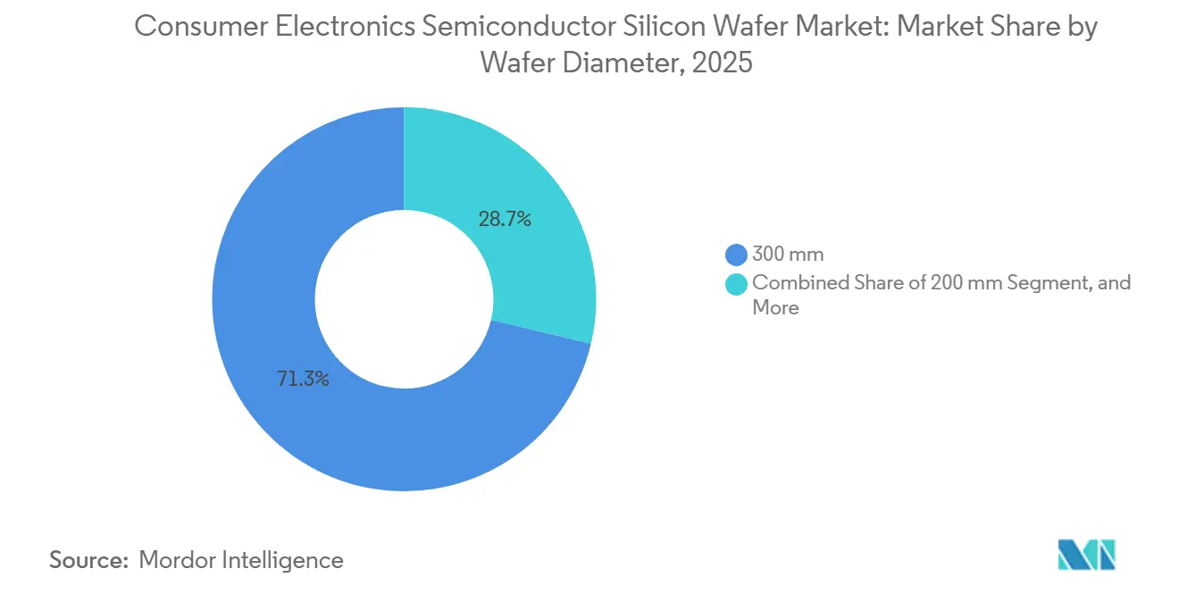
- By wafer diameter, the 300 mm segment commanded 71.29% of the consumer electronics semiconductor silicon wafer market share in 2025 and is forecast to mirror the overall 4.61% CAGR through 2031.
- By semiconductor device type, logic accounted for 42.68% of wafer area in 2025 and is projected to grow at a faster 5.59% CAGR through 2031.
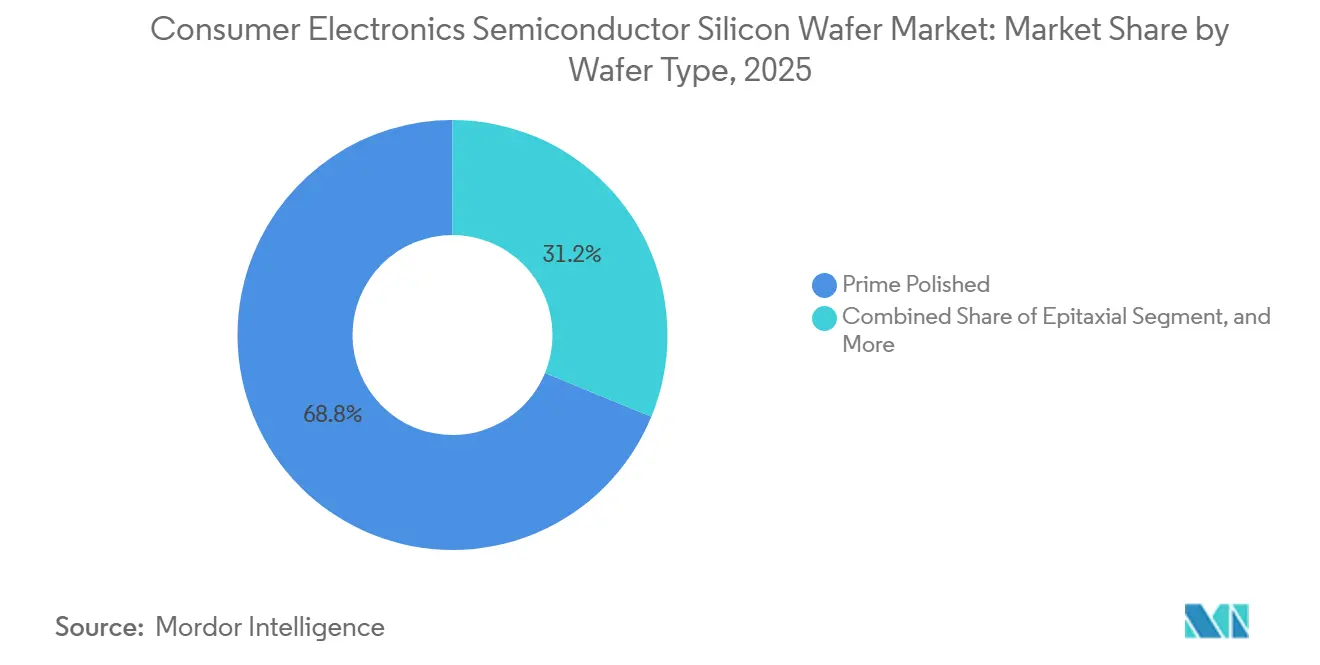
- By wafer type, prime polished substrates accounted for 68.79% of the consumer electronics semiconductor silicon wafer market share in 2025; silicon-on-insulator wafers advance at a 5.31% CAGR through 2031, the highest among wafer grades.
- By geography, Asia-Pacific led with 84.78% volume in 2025 and is on track for a 5.78% CAGR to 2031, outperforming all other regions.
Note: Market size and forecast figures in this report are generated using Mordor Intelligence’s proprietary estimation framework, updated with the latest available data and insights as of January 2026.
Global Consumer Electronics Semiconductor Silicon Wafer Market Trends and Insights
Drivers Impact Analysis*
| Driver | (~) % Impact on CAGR Forecast | Geographic Relevance | Impact Timeline |
|---|---|---|---|
| Proliferation of 5G-Enabled Smartphones | +1.2% | Global, peak adoption in Asia-Pacific and North America | Medium term (2-4 years) |
| Growth in High-Capacity Mobile Storage (3D NAND) | +0.9% | Asia-Pacific core, spillover to North America and Europe | Short term (≤ 2 years) |
| Expansion of Consumer IoT and Wearables | +0.7% | Global, led by North America and Asia-Pacific | Long term (≥ 4 years) |
| Government Incentives for Domestic Logic Fabs | +1.1% | North America, Europe, Japan, India | Medium term (2-4 years) |
| Adoption of TSV Interposers in AR/VR Headsets | +0.5% | North America and Asia-Pacific | Long term (≥ 4 years) |
| Silicon Photonics Uptake in XR Devices | +0.4% | Global, early adoption in North America and Europe | Long term (≥ 4 years) |
| Source: Mordor Intelligence | |||
Proliferation of 5G-Enabled Smartphones
Handset vendors embed multiple sub-6 GHz and millimeter-wave front-end modules, each containing discrete dies for low-noise and power amplifiers. Qualcomm’s Snapdragon 8 Elite, fabricated on an advanced 4 nm process, allocates roughly 30% more wafer area per device than previous LTE platforms. Stand-alone 5G networks are rolling out in China and India, sustaining wafer pull-through even as global unit shipments plateau. Radio-frequency SOI substrates mitigate signal loss, enabling premium pricing that supports the 5.31% CAGR for SOI wafers. Partial substitution by gallium-nitride and indium-phosphide amplifiers tempers, but does not derail, incremental silicon demand.
Growth in High-Capacity Mobile Storage (3D NAND)
Smartphones equipped with 512 GB and 1 TB tiers accelerated a shift to 232-layer NAND stacks, increasing wafer starts and rework cycles. Reported shortages in late 2025 drove an earlier adoption of 1 Tb die schemes, raising silicon consumption per terabyte shipped. Concurrently, Samsung and SK hynix redirected 300 mm lines toward high-bandwidth memory, constricting consumer-grade NAND supply and lifting wafer average selling prices. The resulting demand spike peaks within two years as yield learning curves mature and new capacity comes online.
Expansion of Consumer IoT and Wearables
Smartwatches and fitness trackers integrate application processors, MEMS sensors, and Bluetooth low-energy radios on ultra-low-power nodes. Silicon photonic biosensors, proven to reach sub-nanomolar detection thresholds, underpin next-generation continuous glucose and lactate monitoring.[1]Editorial Team, “Silicon Photonic Biosensors for Continuous Health Monitoring,” NATURE PHOTONICS, nature.com Fabricated on 200 mm and 300 mm wafers, these devices add specialty high-resistivity and sensor-grade substrates to the mix. Adoption scales throughout the decade as privacy safeguards and regulatory frameworks converge, embedding a long-duration lift to wafer demand.
Government Incentives for Domestic Logic Fabs
Public-sector stimulus shapes substrate geography by subsidizing advanced-node fabs. The U.S. CHIPS and Science Act channeled USD 36.4 billion across 40 projects by 2025.[2]U.S. Government Accountability Office, “CHIPS Act: Commerce Has Awarded Billions but Needs to Strengthen Oversight of Grantees,” GAO, gao.gov The EU Chips Act mobilized EUR 80 billion (USD 88 billion) in combined spending, while Japan offered up to JPY 732 billion (USD 4.9 billion) for TSMC’s Kumamoto site. These programs favor prime polished and epitaxial wafers with sub-5 ppm defect densities, anchoring higher-value substrate demand as greenfield fabs ramp over a 2-4 year horizon.
Restraints Impact Analysis*
| Restraint | (~) % Impact on CAGR Forecast | Geographic Relevance | Impact Timeline |
|---|---|---|---|
| Capital-Intensive Large-Diameter Crystal Growth | -0.8% | Global, acute in North America and Europe | Medium term (2-4 years) |
| Supply Constraints of High-Purity Polysilicon | -0.6% | Global, spillover effects in Asia-Pacific | Short term (≤ 2 years) |
| Shift of RF Modules to Compound Substrates | -0.5% | Global, led by North America and Asia-Pacific | Long term (≥ 4 years) |
| Carbon-Footprint Caps from Consumer OEMs | -0.4% | Global, stringent in North America and Europe | Medium term (2-4 years) |
| Source: Mordor Intelligence | |||
Capital-Intensive Large-Diameter Crystal Growth
A single 300 mm Czochralski line can exceed USD 400 million when factoring in pullers, slicing saws, and metrology. Equipment lead times often surpass two years, delaying new capacity during cyclical upswings. Siltronic’s mid-single-digit revenue decline outlook for 2026 underscores how prolonged inventory digestion and deferred capex amplify fixed-cost exposure.[3]Investor Relations, “Financial Reports,” SILTRONIC AG, siltronic.com SUMCO’s planned closure of its Miyazaki 200 mm plant by the end of 2026 reflects legacy overcapacity and the capital burden of retooling. Higher labor and energy costs in North America and Europe further elevate breakeven thresholds, tightening this restraint.
Carbon-Footprint Caps from Consumer OEMs
Apple targets carbon neutrality across its supply chain by 2030, and Samsung aims for net-zero Scope 1 and 2 emissions within the same decade. Silicon wafer production is energy-intensive, demanding continuous high-temperature processes. Soitec invested in on-site renewable energy and efficiency upgrades at its Bernin plant to comply with customer mandates, reallocating funds away from expansion. Such decarbonization spending compresses margins without proportional pricing relief, applying a medium-term drag to growth.
*Our forecasts treat driver/restraint impacts as directional, not additive. The impact forecasts reflect baseline growth, mix effects, and variable interactions.
Segment Analysis
By Wafer Diameter: 300 mm Platforms Sustain Dominance
The 300 mm class captured 71.29% of the consumer electronics semiconductor silicon wafer market share in 2025, reflecting superior die-per-wafer economics that outweigh higher tool costs. This segment follows a growth curve aligned with the overall 4.61% CAGR as foundries channel record capex toward 3 nm and gate-all-around nodes. TSMC alone earmarked USD 52-56 billion for 2026 expansions, nearly all of which were devoted to 300 mm fabs. The consumer electronics semiconductor silicon wafer market size for 300 mm platforms is poised to reach 4,900 million square inches by 2031.
Emerging thinning and bonding techniques enable 300 mm substrates below 50 µm, unlocking applications once restricted to smaller diameters. Meanwhile, 200 mm lines persist for analog, MEMS, and power discretes, where process migration delivers limited benefit. Sub-150-mm wafers are receding to niche roles, chiefly high-resistivity RF switches and specialty sensors. Supply rationalization, including SUMCO’s Miyazaki shutdown, helps stabilize pricing for legacy nodes even as premium 300 mm output scales.


By Semiconductor Device Type: Logic Leads Growth Trajectory
Logic devices consumed 42.68% of wafer area in 2025, outpacing other segments and on track for a 5.59% CAGR through 2031. Smartphone application processors, graphics engines, and on-device AI accelerators collectively stretch die sizes, driving wafer demand. By 2031, the logic segment of the consumer electronics semiconductor silicon wafer market is projected to expand to an impressive 3,000 million square inches.
Memory’s share moderates as Samsung and SK hynix divert capacity toward high-bandwidth DRAM for datacenter accelerators, moving wafer starts away from consumer NAND. Analog and discrete devices sustain incremental gains enabled by Internet-of-Things sensors and power management ICs, but remain tethered to mature 40 nm nodes. Optoelectronics, powered by silicon photonics research successes, could enlarge its footprint later in the decade if monolithic integration achieves cost parity.
By Wafer Type: SOI Outpaces Mainstream Grades
Prime polished wafers held 68.79% share in 2025 and remain the workhorse for logic and memory fabrication. Yet SOI substrates post a 5.31% CAGR through 2031, the fastest among wafer types, propelled by radio-frequency front-end modules and emerging edge-AI accelerators. By the end of the forecast period, SOI's share in the consumer electronics semiconductor silicon wafer market could exceed 12%, driven by increasing adoption of advanced technologies and growing demand for high-performance electronic devices.
Soitec’s EUR 830 million (USD 913 million) fiscal 2024-2025 revenue and its planned EUR 800-850 million (USD 880-935 million) fiscal 2025-2026 guidance illustrate healthy specialty demand despite a cyclical lull. Epitaxial wafers remain relevant for power transistors up to 100 W, while high-resistivity and sensor-grade substrates serve 5G mmWave switches and wearable biosensors, respectively. Compound-substrate encroachment in RF amplifiers constrains total silicon volume but lifts blended ASPs for the residual mix.
Geography Analysis
Asia-Pacific led the consumer electronics semiconductor silicon wafer market share with 84.78% of 2025 volume and is advancing at a 5.78% CAGR through 2031. The region benefits from deep supply chains in Taiwan, South Korea, Japan, and China, each supported by multi-billion-dollar incentives for advanced logic fabs. TSMC’s heavy 2026 capital program and China’s goal of holding one-quarter of global 12-inch capacity further anchor demand. South Korean firms are pivoting 300 mm lines to high-bandwidth memory, tightening local supply for commodity NAND. India’s USD 10 billion semiconductor mission brings new proposals, yet wafer production there still relies on imports.
North America is growing from a low base as the CHIPS and Science Act channels USD 36.4 billion into fab construction. TSMC’s Arizona complex and Intel’s Ohio project will stimulate local substrate pull once high-volume manufacturing begins in 2027. GlobalWafers plans the first U.S. 300 mm wafer plant in two decades, but higher labor and power costs temper its cost position. Europe mobilized EUR 80 billion under the EU Chips Act, focusing on analog and power devices in Germany and France. Siltronic’s revenue outlook points to continued inventory digestion, yet regional funding should slow the talent drain to Asia.
South America, the Middle East, and Africa together account for only a sliver of the consumer electronics semiconductor silicon wafer market size because they lack large crystal-growth facilities. These regions depend on imports from Asia and, to a lesser extent, Europe and the United States. Global ISO 9001 and ISO 14001 standards maintain product quality consistency, but geographic concentration still exposes the supply chain to natural disasters and geopolitical tensions.

Competitive Landscape
Five suppliers, Shin-Etsu Chemical, SUMCO, GlobalWafers, Siltronic, and SK Siltron, account for most 300 mm prime-polished output, giving them scale advantages in crystal growth and polishing. Their combined grip fosters moderate concentration, yet price competition remains active because customers dual-source critical nodes. Vertical integration into polysilicon lets Shin-Etsu and SUMCO cushion input swings, while GlobalWafers focuses on geographic risk diversification.
Incumbents are adjusting capacity to rebalance supply. TSMC’s record capex secures long-term orders, but wafer makers still face near-term softness at mature nodes. SUMCO will shutter its Miyazaki 200 mm plant by late 2026, helping to cut trailing-edge oversupply. Siltronic projects a mid-single-digit revenue decline for 2026 as inventory digestion lingers. Capital discipline and selective tool upgrades dominate strategic plans until demand visibility improves.
New players and niche specialists add competitive pressure. Chinese state-supported firms such as National Silicon Industry Group and Zhonghuan Semiconductor are scaling 12-inch lines to serve domestic customers seeking a secure supply. Soitec is expanding its capacity in Singapore for silicon-on-insulator wafers used in radio-frequency front-end modules. Reclaimed wafer vendors like Phoenix Silicon International pitch circular-economy value, appealing to consumer brands with strict carbon targets. Technology differentiation centers on defect density, flatness, and contamination control, metrics that directly affect advanced-node yield.
Consumer Electronics Semiconductor Silicon Wafer Industry Leaders
Shin-Etsu Chemical Co., Ltd.
SUMCO Corporation
GlobalWafers Co., Ltd.
Siltronic AG
SK siltron Co., Ltd.
- *Disclaimer: Major Players sorted in no particular order

Recent Industry Developments
- February 2026: TSMC disclosed USD 52-56 billion 2026 capex focused on 300 mm expansions in Taiwan, Japan and Arizona.
- December 2025: Soitec announced new 300 mm SOI capacity in Singapore with fiscal 2025-2026 revenue guidance of EUR 800-850 million (USD 880-935 million).
- November 2025: SUMCO revealed plans to shutter its Miyazaki 200 mm plant by end-2026.
- October 2025: GlobalWafers committed to a 300 mm Texas fab pending CHIPS Act incentives.


Global Consumer Electronics Semiconductor Silicon Wafer Market Report Scope
The Consumer Electronics Semiconductor Silicon Wafer Market Report is Segmented by Wafer Diameter (Up to 150 mm, 200 mm, 300 mm), Semiconductor Device Type (Logic, Memory, Analog, Discrete, Other Semiconductor Device Types), Wafer Type (Prime Polished, Epitaxial, Silicon-on-Insulator (SOI), Specialty Silicon), and Geography (North America, Europe, Asia-Pacific, South America, Middle East, Africa). The Market Forecasts are Provided in Terms of Shipment Volume (Square Inches).
| Up to 150 mm |
| 200 mm |
| 300 mm |
| Logic |
| Memory |
| Analog |
| Discrete |
| Other Semiconductor Device Types (Optoelectronics, Sensors, Micro) |
| Prime Polished |
| Epitaxial |
| Silicon-on-Insulator (SOI) |
| Specialty Silicon (High-Resistivity, Power, Sensor-Grade) |
| North America | United States |
| Canada | |
| Mexico | |
| Europe | Germany |
| United Kingdom | |
| France | |
| Rest of Europe | |
| Asia-Pacific | China |
| Japan | |
| India | |
| South Korea | |
| Taiwan | |
| Rest of Asia-Pacific | |
| South America | |
| Middle East | |
| Africa |
| By Wafer Diameter | Up to 150 mm | |
| 200 mm | ||
| 300 mm | ||
| By Semiconductor Device Type | Logic | |
| Memory | ||
| Analog | ||
| Discrete | ||
| Other Semiconductor Device Types (Optoelectronics, Sensors, Micro) | ||
| By Wafer Type | Prime Polished | |
| Epitaxial | ||
| Silicon-on-Insulator (SOI) | ||
| Specialty Silicon (High-Resistivity, Power, Sensor-Grade) | ||
| By Geography | North America | United States |
| Canada | ||
| Mexico | ||
| Europe | Germany | |
| United Kingdom | ||
| France | ||
| Rest of Europe | ||
| Asia-Pacific | China | |
| Japan | ||
| India | ||
| South Korea | ||
| Taiwan | ||
| Rest of Asia-Pacific | ||
| South America | ||
| Middle East | ||
| Africa | ||


Key Questions Answered in the Report
What is the projected volume for the consumer electronics semiconductor silicon wafer market by 2031?
The market is forecast to reach 6.83 billion square inches by 2031.
Which wafer diameter dominates shipments to consumer electronics fabricators?
300 mm substrates led with 71.29% share in 2025 and will remain the primary format through 2031.
How quickly are logic device wafers growing compared with memory wafers?
Logic wafers expand at a 5.59% CAGR from 2026-2031, outpacing memory as AI-centric processors proliferate.
Why are SOI wafers gaining share in smartphone components?
Radio-frequency SOI’s high resistivity improves signal integrity in 5G front-end modules, driving a 5.31% CAGR for SOI volumes.
Which region contributes the most wafer demand for consumer electronics?
Asia-Pacific supplied 84.78% of volume in 2025 and remains the fastest-growing region at a 5.78% CAGR.
How are environmental targets influencing wafer suppliers?
Carbon-neutrality mandates from brands such as Apple force suppliers to invest in renewable energy and efficiency upgrades, increasing cost structures.
Page last updated on:


