China LED Epitaxial Wafer Market Size and Share
Market Overview
| Study Period | 2020 - 2031 |
|---|---|
| Forecast Data Period | 2026 - 2031 |
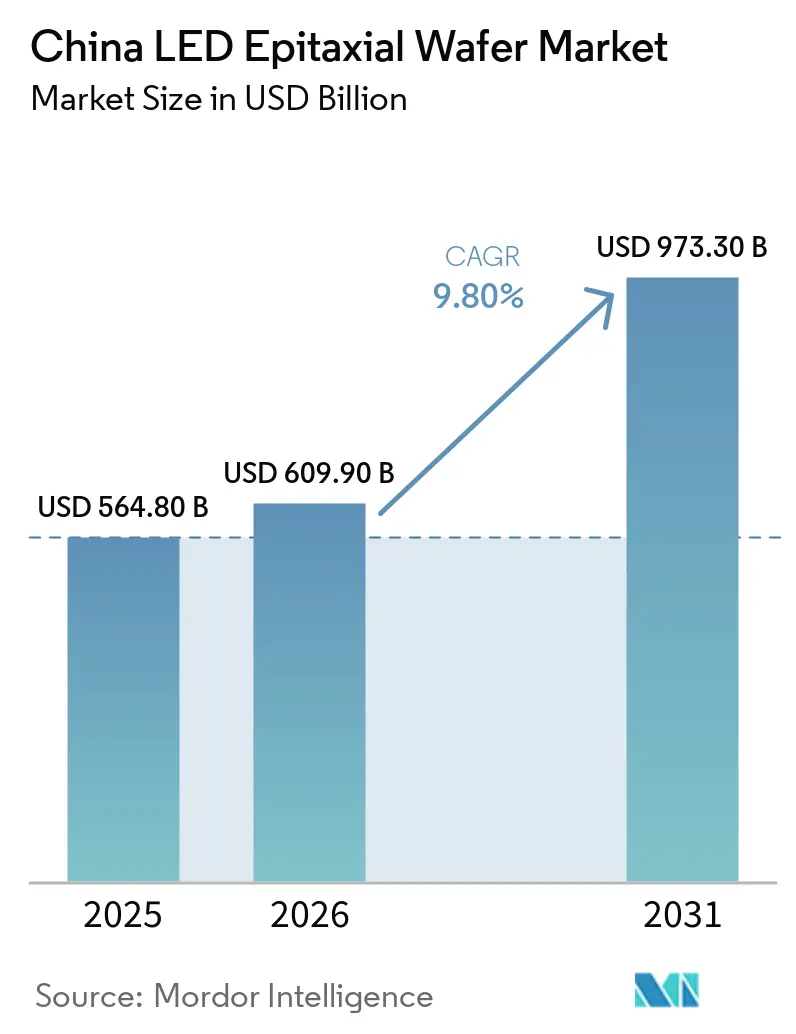
| Base Year Market Size (2025) | USD 564.80 Billion |
| Market Size (2026) | USD 609.90 Billion |
| Market Size (2031) | USD 973.30 Billion |
| Growth Rate (2026 - 2031) | 9.80% CAGR |
| Market Concentration | Medium |
Major Players *Disclaimer: Major Players sorted in no particular order Image © Mordor Intelligence. Reuse requires attribution under CC BY 4.0. | |
China LED Epitaxial Wafer Market Analysis by Mordor Intelligence
The China LED epitaxial wafer market size is projected to be USD 564.8 million in 2025, USD 609.9 million in 2026, and reach USD 973.3 million by 2031, growing at a CAGR of 9.8% from 2026 to 2031. Powerful tailwinds come from panel makers’ shift to mini-LED backlights, automakers’ appetite for adaptive matrix lamps, and government incentives that steer investment into display-grade and automotive-qualified wafers. GaN technology remains the volume engine, yet rapid adoption of AlGaN for deep-ultraviolet sterilization and GaN-on-silicon for 200 mm lines signals a bifurcation between commodity and value-added segments. Capacity is tightly clustered in East and Central China, giving leading players scale economics while second-tier firms face yield challenges and capital fatigue. Cost-per-die pressure in consumer displays is accelerating the 200 mm transition, whereas reliability demands in vehicles and UVC modules preserve space for 150 mm sapphire production.
Key Report Takeaways
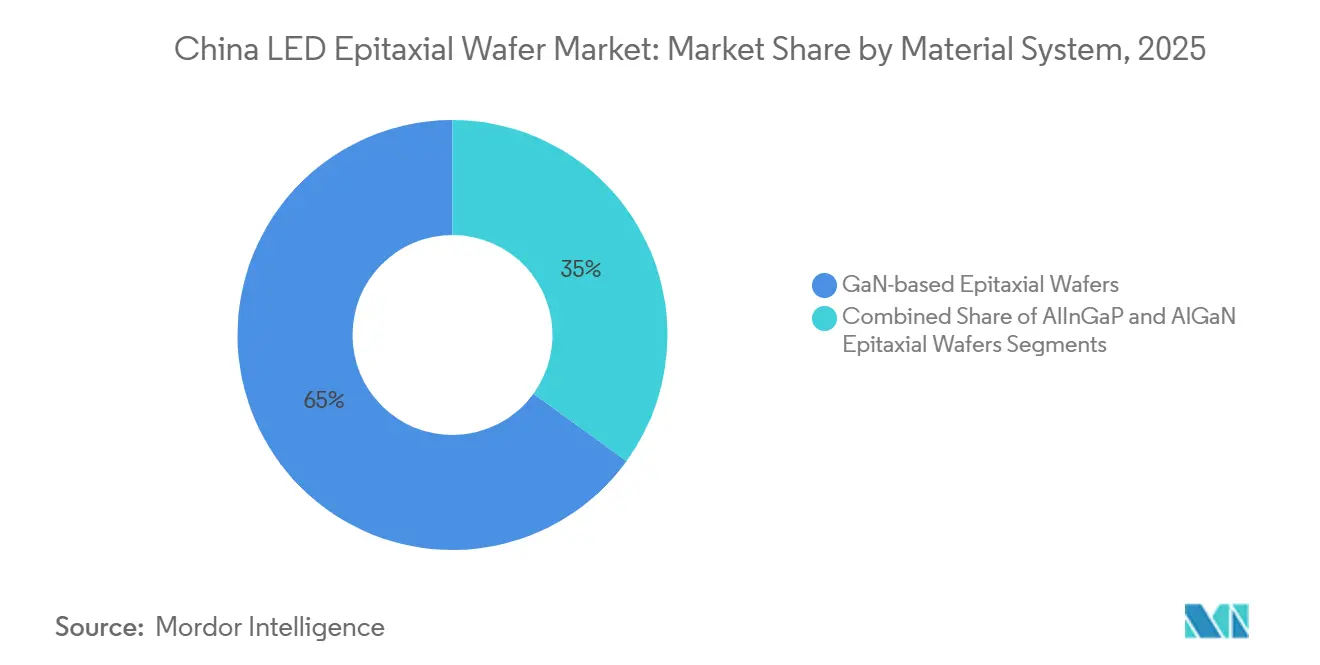
- By material system, GaN-based wafers led with 65% revenue share in 2025, while AlGaN is projected to expand at a 12.34% CAGR through 2031.
- By substrate type, sapphire commanded 55.63% share in 2025; silicon platforms are forecast to grow at a 13.3% CAGR to 2031.
- By wafer diameter, the 150 mm format captured 43.24% of value in 2025, whereas 200 mm and above wafers are poised for a 14.24% CAGR over 2026-2031.
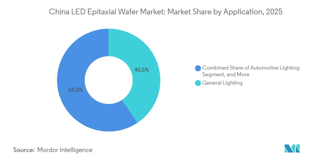
- By application, general lighting held a 40.54% share of the China LED epitaxial wafer market size in 2025, and displays and backlighting are advancing at a 13.59% CAGR through 2031.
Note: Market size and forecast figures in this report are generated using Mordor Intelligence’s proprietary estimation framework, updated with the latest available data and insights as of January 2026.
China LED Epitaxial Wafer Market Trends and Insights
Drivers Impact Analysis*
| DRIVER | (~) % IMPACT ON CAGR FORECAST | GEOGRAPHIC RELEVANCE | IMPACT TIMELINE |
|---|---|---|---|
| Rapid Expansion of Mini and Micro LED Display Manufacturing Lines | +2.80% | East China, Central China, spillover to South Central China | Medium term (2-4 years) |
| Government Subsidies and Tax Incentives for Domestic LED Supply Chain | +1.90% | National, concentrated in East and Central China | Long term (≥4 years) |
| Energy Efficiency Mandates Driving LED Adoption in General Lighting | +1.20% | Nationwide, led by East and North China cities | Medium term (2-4 years) |
| Accelerated Automotive LED Penetration in New Energy Vehicles | +1.60% | Nationwide, early gains in East and South Central China | Short term (≤2 years) |
| Rising Demand for UVC LED Epitaxial Wafers for Water Purification | +0.90% | East China manufacturing, export to Southeast Asia | Medium term (2-4 years) |
| Localization Push for Silicon Carbide Substrate Supply Security | +0.70% | East, North, and Southwest China | Long term (≥4 years) |
| Source: Mordor Intelligence | |||
Government Subsidies And Tax Incentives For Domestic LED Supply Chain
The 14th Five-Year Plan tilts subsidies toward advanced nodes rather than sheer volume, cutting effective capital costs for 200 mm GaN-on-Si and AlGaN reactors by up to 30%. Provincial programs in Xiamen and Wuhan layer land concessions and utility discounts that shave operating expenses by 10-15%, accelerating breakeven for new fabs.[2]Ministry of Industry and Information Technology, “14th Five-Year Plan,” miit.gov.cn Conditions now require 70% domestic equipment content by 2027, funneling orders to local MOCVD vendors such as AMEC and protecting strategic know-how. The policy mix reduces payback periods, sustains R&D outlays despite thinning chip margins, and lengthens the runway for premium-grade wafer expansion through 2031.
Energy Efficiency Mandates Driving LED Adoption In General Lighting
China’s carbon-neutral pledge turns building retrofits into a structural floor of demand. Standard GB 50034-2024 lifts minimum efficacy thresholds to 110-130 lm/W, rendering legacy fluorescent fixtures non-compliant and triggering mandated upgrades in government facilities.[3]Standardization Administration of China, “GB 50034-2024,” sac.gov.cnMunicipal rebates reimburse up to 40% of retrofit costs, bringing forward replacement cycles and sustaining baseline wafer shipments even amid commoditization. Residential smart bulbs add incremental pull by requiring dual-chip or RGB wafers for tunable white solutions. This driver ensures the China LED epitaxial wafer market continues to harvest steady lighting demand while shifting capex toward display and vehicle segments.
Accelerated Automotive LED Penetration In New Energy Vehicles
A 51% new-energy vehicle sales mix in 2025 forces automakers to differentiate through lighting aesthetics and safety, driving adoption of adaptive matrix headlamps and ambient strips. BYD, NIO, and Li Auto now specify AEC-Q102-qualified dies with ≤2 nm wavelength spread, premiums that run 40-50% above general-lighting chips yet lock in multiyear supply contracts. Tier-1 system integrators localize sourcing to avoid tariff risk, shortening development cycles and embedding Chinese wafer makers deeper into international auto supply chains. The result is a resilient, high-margin demand stream that balances volatile commodity segments.
Restraints Impact Analysis*
| RESTRAINT | (~) % IMPACT ON CAGR FORECAST | GEOGRAPHIC RELEVANCE | IMPACT TIMELINE |
|---|---|---|---|
| High Capital Intensity and Depreciation of MOCVD Equipment | -1.40% | National, hardest on second-tier players in North and Southwest China | Short term (≤2 years) |
| Price Erosion Due to Overcapacity in Conventional LED Chips | -2.10% | Nationwide, acute in East and South Central clusters | Short term (≤2 years) |
| Technical Yield Challenges in 200 mm GaN-on-Si Platforms | -0.80% | East and Central China | Medium term (2-4 years) |
| Environmental Regulations on Ammonia and Arsine Emissions Limiting Expansion | -0.60% | Nationwide, strictest in coastal metros | Long term (≥4 years) |
| Source: Mordor Intelligence | |||
Rapid Expansion Of Mini And Micro LED Display Manufacturing Lines
Display giants are tying wafer supply directly to panel roadmaps, locking in long-term offtake agreements that pull 6-inch and 200 mm capacity toward RGB and high-uniformity blue products. TCL CSOT’s acquisition of Prima secures back-end integration and creates stable demand for wafers that meet sub-3 nm wavelength targets.[1]TCL CSOT, “Acquires Prima to Strengthen Mini-LED Chain,” tclcsot.comSanan more than quintupled monthly microLED wafer output across 2024-2025, qualifying for Samsung’s flagship televisions and proving Chinese vendors can hit premium uniformity benchmarks. HC Semitek’s Zhuhai fab adds 3,000 six-inch wafers a month of incremental volume, synchronized with BOE’s USD 3 billion Gen 8.6 backlight investments. Together, these moves anchor medium-term growth, lifting utilization at leading fabs and absorbing oversupply from general-lighting lines.
Price Erosion Due To Overcapacity In Conventional LED Chips
Installed blue-chip capacity exceeded demand by roughly 30% in 2025, slicing average wafer prices 12-15% year-over-year. Commodity 2835 packages fell 18%, pushing general-lighting wafer makers into a margin squeeze that drains resources for R&D. Clustered mid-sized producers in Xiamen, Shenzhen, and Zhongshan compete for identical lighting contracts, often awarded quarterly, deepening volatility. Profit-oriented niche specialists such as Changelight sidestep the spiral by pivoting to automotive and horticulture, but the broader base endures a persistently deflationary environment that weighs on the China LED epitaxial wafer market.
High Capital Intensity And Depreciation Of MOCVD Equipment
Six-inch GaN reactors cost USD 3.5 million, and 200 mm tools exceed USD 5 million, with installation and qualification adding a further 30%. Assets bought during the 2018-2020 boom are nearing full amortization, putting pressure on cash flows just as new display-grade tools must be ordered.[4]Aixtron SE, “MOCVD Specifications,” aixtron.comHC Semitek’s first-half 2025 net loss illustrates the strain of servicing USD 700 million in project debt while yields ramp. Smaller firms sitting below 60% utilization defer purchases, slowing process migration, and reinforcing scale advantages for incumbents.
*Our forecasts treat driver/restraint impacts as directional, not additive. The impact forecasts reflect baseline growth, mix effects, and variable interactions.
Segment Analysis
By Material System: GaN Strength Funds AlGaN’s UVC Upswing
GaN-based wafers captured 65% of the 2025 value, underpinned by blue emission for phosphor-converted white lamps, RGB backlights, and automotive headlamps. Stable volumes from lighting and displays mean this segment continues to anchor cash flow and subsidize R&D. AlGaN supplies only a fraction of present output, yet health-sector regulations banning mercury lamps and rising demand for point-of-use sterilization enable a 12.34% CAGR that materially outpaces the China LED epitaxial wafer market size as a whole. Sanan’s USD 950 million multiyear build-out, plus pilot lines at Hubei DUVTek, signal that China aims to displace imports and own the deep-UV value chain. Secondary AlInGaP lines serve automotive brake lights and horticulture, giving fabs a hedge against blue-chip cyclicality.
Commercial acceptance of wafer-scale AlGaN rides on recent breakthroughs pushing external quantum efficiency near 10%, opening export prospects to Southeast Asian water utilities. Domestic municipal tenders increasingly stipulate solid-state UVC, locking in a durable demand baseline. Taken together, the portfolio effect of GaN dominance and AlGaN growth stabilizes revenue, ensuring the China LED epitaxial wafer market can bankroll process innovations without jeopardizing near-term earnings.


By Substrate Type: Sapphire Maturity Versus Silicon Disruption
Sapphire commanded a 55.63% share in 2025 thanks to lattice compatibility, an established 8-inch supply, and familiarity among automotive OEMs. Its proven reliability preserves design-in status for headlamps and outdoor fixtures even as price pressure mounts in lighting. Silicon-based GaN is the natural challenger, offering a larger 200 mm diameter, lower raw-wafer cost, and compatibility with existing CMOS fabs, underpinning a 13.3% CAGR that overtakes sapphire growth. The China LED epitaxial wafer market share for silicon rises fastest where panel makers chase bill-of-materials savings, particularly in mini-LED backlighting.
Process maturity remains the gating factor. Edge-related forward-voltage drift on 200 mm GaN-on-Si still reduces usable die area, but partnerships such as ALLOS-Ennostar promise sub-3% wavelength uniformity, a threshold that unlocks bin-free mass transfer. Silicon carbide fills niche power and high-temperature roles, overlapping with EV drive-train inverters and offering cross-utilization of crystal growth know-how. The substrate mix therefore evolves toward a dual-track structure, with sapphire safeguarding stringent reliability markets and silicon harvesting high-volume consumer displays.
By Wafer Diameter: 150 mm Incumbency Slows 200 mm Adoption
The 150 mm format retained 43.24% value in 2025 by virtue of sunk capital, qualified automotive designs, and higher usable die area than early 200 mm runs. Its entrenched tooling keeps average depreciation low, allowing producers to price aggressively in commodity lighting while funding premium lines. The 200 mm cohort, however, carries the fastest growth at 14.24% CAGR as BOE, TCL CSOT, and Samsung demand higher die density per reactor cycle to claw down mini-LED backlight cost. The China LED epitaxial wafer market size for 200 mm products expands as yields inch upward and transfer-print houses certify larger-diameter wafers.
Yield drag still lurks, especially in the outer 10 mm annulus, where thermal gradients spike dislocation density. Producers mitigate losses by rerouting edge dice to low-tier products, but true economic parity hinges on front-end process tweaks now under joint development with equipment makers. Until then, most new display lines run parallel 6-inch sapphire and 200 mm silicon reactors, hedging risk while sustaining supply flexibility.
By Application: Lighting Cash Flow Fuels Display And Vehicle Upside
General lighting delivered 40.54% revenue in 2025, driven by building-retrofit mandates that guarantee a recurring replacement cycle as decade-old bulbs reach end-of-life. Although unit ASPs erode, the sheer shipment scale maintains wafer absorptive capacity. Displays and backlighting record the sharpest ascent, registering a 13.59% CAGR on the back of television and tablet launches requiring 5,000-25,000 mini-LEDs apiece, outpacing the broader China LED epitaxial wafer market. Automotive lighting stands as a strategic profit pool, with adaptive headlamps and ambient strips priced at 30-50% premiums and cemented by multiyear vehicle programs.
UV sterilization remains a small base, yet logs triple-digit growth bursts when municipal tenders deploy mercury-free systems. Industrial and specialty lighting adds steady mid-single-digit increments, anchored by horticulture and machine-vision niches that value custom wavelength bins. The net effect is a healthy mix where mature lighting volumes stabilize factory utilization while high-spec display and vehicle applications elevate blended margins.
Geography Analysis
East China concentrates roughly 70% of reactors across Xiamen, Yangzhou, and surrounding cities, leveraging proximity to sapphire substrate makers and panel assemblers along the Pearl and Yangtze River deltas. Sanan Optoelectronics and Changelight anchor Xiamen’s Torch zone, capturing scale benefits in utilities, logistics, and shared MOCVD service networks that lower cost per wafer versus inland peers. Panel majors in Shenzhen and Guangzhou create a natural pull, allowing same-day shipment of display-grade wafers and reinforcing the China LED epitaxial wafer market’s center-of-gravity on the southeast coast.
Central China is the emergent growth pole, with Wuhan’s East Lake zone courting USD 1.8 billion in Sanan investment and NationStar’s RGB lines in Nanchang clustering around automotive OEMs in Hubei and Jiangxi. Lower land and labor costs, plus direct rail links to coastal ports, spur reactor installations that outpace the national average. South Central China, dominated by Guangdong, hosts the densest packaging and module assembly ecosystem, and HC Semitek’s Zhuhai fab marks a deliberate strategy to co-locate front-end and back-end assets for panel customers, shortening cycle times.
North China provides R&D heft through university labs in Beijing and pilot 200 mm GaN-on-Si lines, yet high operating costs curb mass deployment. Southwest China retains legacy capacity built on earlier subsidy waves, but under-utilization persists due to distance from major downstream buyers. Northwest and Northeast regions remain peripheral, hosting only small-scale demo lines tied to academic institutes. The geographic mosaic underscores how policy incentives, substrate supply, and customer vicinity converge to favor coastal clusters within the China LED epitaxial wafer market.
Competitive Landscape
Sanan Optoelectronics towers over rivals with roughly 60% of national capacity, yet the China LED epitaxial wafer market stays moderately contested as HC Semitek, Changelight, Focus Lightings, and Elec-Tech jointly lift top-five share to about 80%. Price pressure in blue-chip lighting prevents any single firm from wielding pricing power, compelling differentiation through integration, node leadership, or niche specialization. BOE’s USD 285 million control of HC Semitek secures captive wafers for its backlight lines, mirroring how Samsung aligned with Sanan for microLED television supply. Sanan’s USD 239 million takeover of Lumileds injects automotive-grade packaging IP and entrée into European Tier-1 channels, widening its moat.
Technology races cluster around 200 mm GaN-on-Si yield, AlGaN external quantum efficiency, and microLED wavelength uniformity. The January 2026 ALLOS-Ennostar pact to co-develop 200 mm platforms illustrates a pivot from capacity scaling to process finesse. Smaller firms survive by focusing on horticulture or industrial wavelengths where rapid prototyping trumps sheer volume; Changelight’s 88% profit surge in first-half 2025 validates the strategy. Equipment vendors such as AMEC benefit from domestic content rules, capturing reactor orders that once flowed to foreign suppliers and reinforcing a semi-closed loop that underpins supply-chain resilience.
Despite concentration at the top, the absence of binding long-term contracts in commodity lighting, coupled with the threat of rapid capacity adds in subsidized zones, keeps profit pools in flux. Consolidation pressures build on second-tier producers who lack display-panel or automotive anchors, suggesting further M&A or attrition by 2028. Collectively, these dynamics sustain a market where scale, technology, and captive demand dictate staying power.
China LED Epitaxial Wafer Industry Leaders
Sanan Optoelectronics Co., Ltd.
HC Semitek Corporation
Focus Lightings Tech Co., Ltd.
Elec-Tech International Co., Ltd.
NationStar Optoelectronics Co., Ltd.
- *Disclaimer: Major Players sorted in no particular order

Recent Industry Developments
- January 2026: ALLOS Semiconductors and Ennostar partnered to scale 200 mm GaN-on-Si epitaxial wafers, targeting sub-3% wavelength uniformity.
- January 2026: TCL CSOT acquired Prima for RMB 490 million (USD 67.6 million), locking in module capacity for mini-LED monitors.
- August 2025: Sanan Optoelectronics closed its USD 239 million purchase of Lumileds, adding automotive packaging expertise.
- March 2025: HC Semitek began mass production at its USD 700 million Zhuhai microLED wafer fab, aiming for 3,000 six-inch wafers monthly by year-end.


China LED Epitaxial Wafer Market Report Scope
| GaN-based Epitaxial Wafers |
| AlInGaP Epitaxial Wafers |
| AlGaN Epitaxial Wafers |
| Sapphire |
| Silicon |
| Silicon Carbide (SiC) |
| Gallium Arsenide (GaAs) |
| Up to 100 mm |
| 150 mm |
| 200 mm and Above |
| General Lighting |
| Automotive Lighting |
| Displays and Backlighting |
| UV Sterilization |
| Industrial and Specialty Lighting |
| By Material System | GaN-based Epitaxial Wafers |
| AlInGaP Epitaxial Wafers | |
| AlGaN Epitaxial Wafers | |
| By Substrate Type | Sapphire |
| Silicon | |
| Silicon Carbide (SiC) | |
| Gallium Arsenide (GaAs) | |
| By Wafer Diameter | Up to 100 mm |
| 150 mm | |
| 200 mm and Above | |
| By Application | General Lighting |
| Automotive Lighting | |
| Displays and Backlighting | |
| UV Sterilization | |
| Industrial and Specialty Lighting |


Key Questions Answered in the Report
What is the projected value of the China LED epitaxial wafer market by 2031?
The market is forecast to reach USD 973.3 million by 2031, up from USD 609.9 million in 2026, reflecting a 9.8% CAGR over 2026-2031.
Which material system dominates current production?
GaN-based wafers hold the largest share at 65% of 2025 revenue thanks to blue and white LED applications.
Why are 200 mm wafers gaining momentum?
Panel makers seek lower cost per die for mini-LED backlights, and advances in GaN-on-Si uniformity are improving 200 mm yields.
How are government policies affecting capacity expansion?
Subsidies now focus on advanced nodes, cutting capital costs by up to 30% for 200 mm and AlGaN reactors and encouraging domestic equipment adoption.
Which end-use segment shows the fastest growth?
Displays and backlighting lead with a projected 13.59% CAGR through 2031 as televisions and tablets shift to mini-LED architectures.
Page last updated on:


