Broad Ion Beam Technology Market Size and Share
Market Overview
| Study Period | 2019 - 2030 |
|---|---|
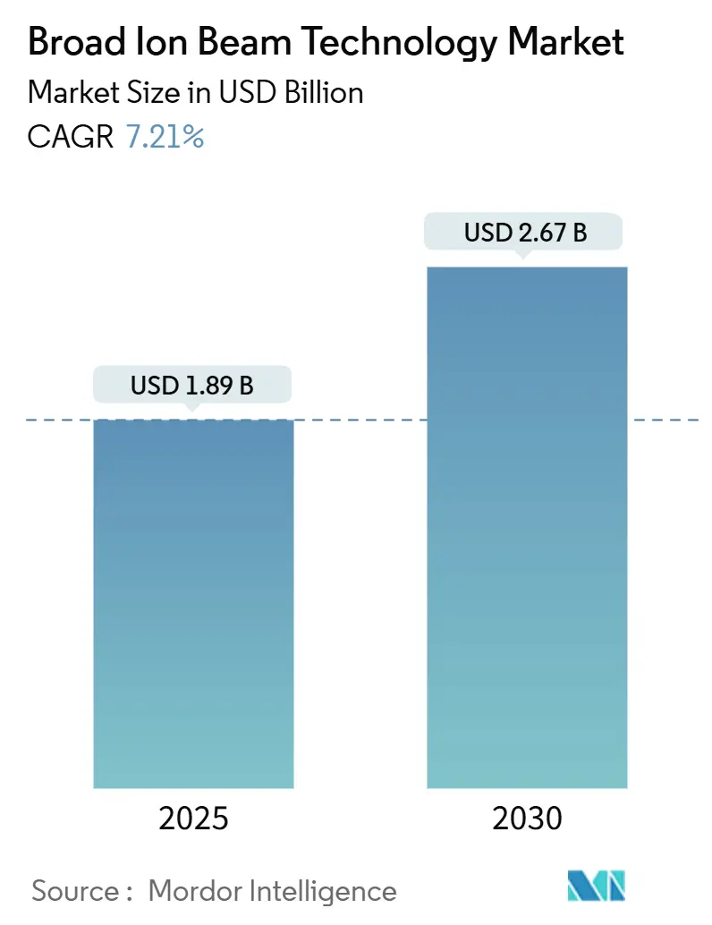
| Market Size (2025) | USD 1.89 Billion |
| Market Size (2030) | USD 2.67 Billion |
| Growth Rate (2025 - 2030) | 7.21% CAGR |
| Fastest Growing Market | Middle East |
| Largest Market | Asia Pacific |
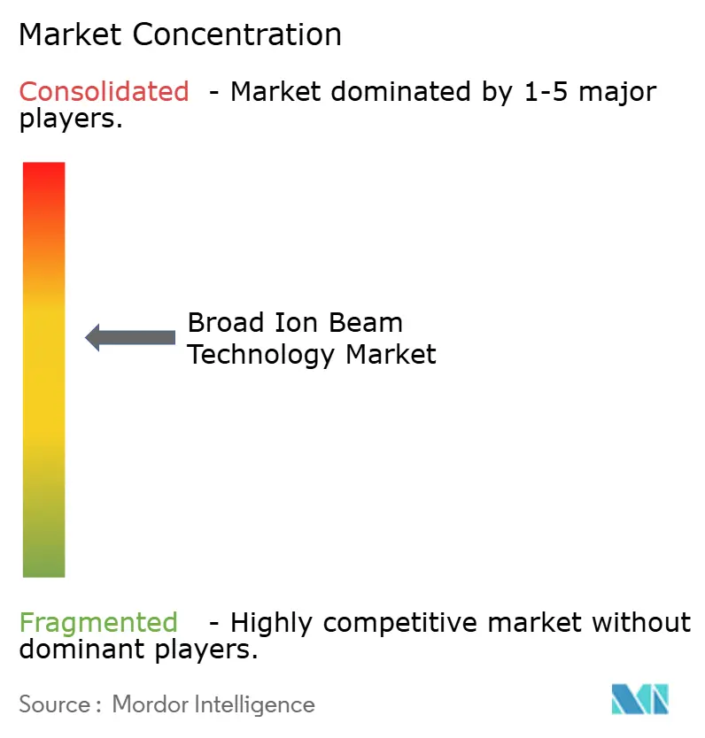
| Market Concentration | Medium |
Major Players *Disclaimer: Major Players sorted in no particular order Image © Mordor Intelligence. Reuse requires attribution under CC BY 4.0. | |
Broad Ion Beam Technology Market Analysis by Mordor Intelligence
The Broad Ion Beam Technology market size is estimated at USD 1.89 billion in 2025 and is projected to reach USD 2.67 billion by 2030, growing at a 7.21% CAGR over the forecast period. Sustained fab expansion, particularly the 103 new 300 millimeter facilities that SEMI expects to go online between 2023 and 2027, is driving demand for sample-preparation and defect-review tools that achieve atomic-scale precision. Integrated device manufacturers are adopting broad ion beam delayering systems to investigate gate-all-around transistors and 3D NAND stacks that photolithography alone cannot expose without damage. Meanwhile, xenon plasma-focused ion beam platforms deliver high currents for rapid lamella fabrication, which is critical to cryo-electron microscopy and advanced packaging workflows. Capital spending on 300 millimeter equipment is projected to climb to USD 137 billion by 2027, reinforcing the Broad Ion Beam Technology market’s mid-single-digit growth trajectory. Adoption is also accelerating in quantum-device fabrication, where deterministic single-ion implantation requires nanometer placement accuracy, demonstrated in peer-reviewed work that reduced residual ²⁹Si to 2.3 ppm, thereby extending electron coherence times into the 10-second regime.
Key Report Takeaways
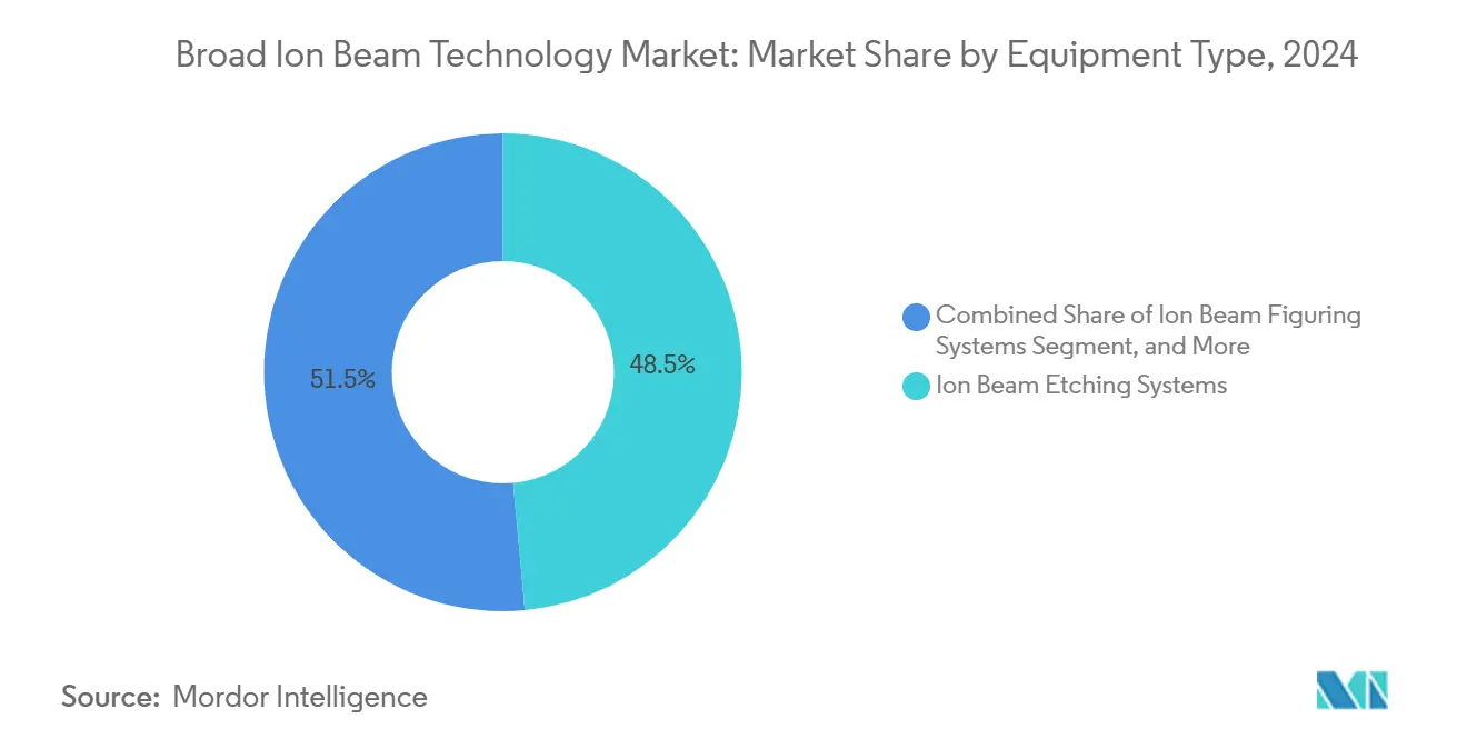
- By equipment type, ion beam etching systems accounted for 48.53% of the revenue in 2024; ion beam figuring tools are projected to expand at a 7.93% CAGR through 2030.
- By ion source type, Kaufman sources accounted for a 39.71% share in 2024, while gas field ion source platforms are poised to grow at a 7.88% CAGR to 2030.
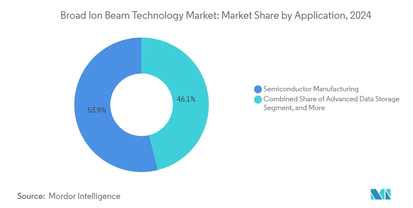
- By application, semiconductor manufacturing led with a 53.89% share in 2024; quantum devices are forecast to post the fastest growth of 8.42% CAGR through 2030.
- By end user, integrated device manufacturers captured 45.22% of the 2024 demand; research institutes are expected to advance at an 8.23% CAGR on the back of national quantum programs.
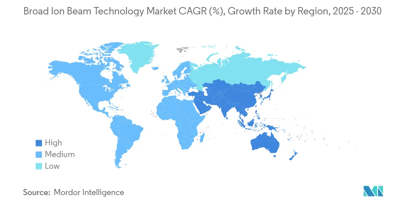
- By geography, the Asia Pacific region dominated with 43.76% of the 2024 revenue; the Middle East is the fastest-growing geography, with an 8.29% CAGR to 2030.
Note: Market size and forecast figures in this report are generated using Mordor Intelligence’s proprietary estimation framework, updated with the latest available data and insights as of January 2026.
Global Broad Ion Beam Technology Market Trends and Insights
Drivers Impact Analysis*
| Driver | (~) % Impact on CAGR Forecast | Geographic Relevance | Impact Timeline |
|---|---|---|---|
| Growing adoption of ion beam milling in semiconductor fabrication | +1.8% | Global, with concentration in Asia Pacific and North America | Medium term (2-4 years) |
| Rising demand for high-resolution TEM sample preparation | +1.5% | Global, particularly Europe and North America research hubs | Short term (≤ 2 years) |
| Expansion of advanced packaging and 3D IC manufacturing | +1.6% | Asia Pacific core, spillover to North America | Medium term (2-4 years) |
| Emergence of defect review integration with AI-enabled ion beam tools | +0.9% | North America and Europe early adopters, Asia Pacific scale deployment | Long term (≥ 4 years) |
| Increasing use of broad ion beams in quantum device nanofabrication | +0.7% | North America, Europe, select Asia Pacific sites (Japan, Singapore) | Long term (≥ 4 years) |
| Shift toward sustainable ion source gases to reduce PFAS emissions | +0.6% | Europe and North America regulatory drivers, Asia Pacific following | Long term (≥ 4 years) |
| Source: Mordor Intelligence | |||
Growing Adoption of Ion Beam Milling in Semiconductor Fabrication
Ion beam milling is transitioning from a niche to a mainstream technology as device makers confront materials that reactive ion etching damages. Canon markets energetic etch platforms for magnetoresistive random-access memory stacks where plasma chemistries degrade tunnel magnetoresistance.[1]Canon U.S.A., “Semiconductor Manufacturing Equipment,” usa.canon.com Scientific Reports demonstrated that pulsed-grid ion beams achieve infinite selectivity while preserving extreme-ultraviolet resist masks, validating the method for sub-10-nanometer features. Hitachi High-Tech’s DCR Etch 9060 couples wafer cooling and infrared heating to alternate adsorption and desorption steps, enabling isotropic atom-layer removal in 3-D NAND above 200 layers. With global 300 millimeter capacity rising 8% annually, every new fab requires multiple ion beam tools for process development, cementing the driver’s influence.
Rising Demand for High-Resolution TEM Sample Preparation
Sub-angstrom imaging of gate-all-around transistors and high-bandwidth memory die stacks depends on artefact-free lamellae. A scanning argon broad ion beam system produced 10 millimeter delayered areas with <50 nanometer non-uniformity, cutting time-to-result in half for failure-analysis teams. Xenon plasma-focused ion beam platforms now generate 15-20 cryo-lamellae per 24-hour run with 70-84% success, far surpassing gallium sources.[2]Hae In Kwon et al., “Enhanced Etch Characteristics …,” Scientific Reports, nature.com Higher currents and inert ions reduce amorphous damage, making broad ion beam technology indispensable for both semiconductor and life-science research.
Expansion of Advanced Packaging and 3-D IC Manufacturing
Heterogeneous integration is transforming packaging into an active performance vector, and ion beam tools are essential for exposing copper-copper hybrid bonds and micro-bump voids without mechanical stress. SEMI projects high-bandwidth memory bits to grow 30-40% annually through 2027, thereby multiplying demand for cross-section analysis. Argon broad ion beam polishing removes grinding layers before electron backscatter diffraction, while xenon plasma beams offer high-rate milling of multilayer stacks, together supporting reliability analysis across the packaging value chain.
Emergence of Defect Review Integration with AI-Enabled Ion Beam Tools
Machine learning is being integrated into ion beam workflows to automate endpoint detection and align with digital twins. The European FIT4NANO roadmap prioritizes open APIs and FAIR data for closed-loop control. Hitachi’s SU9000II SEM provides automatic optics adjustment to accelerate cross-section analysis, and SEMI’s Smart Data-AI initiative is pushing predictive maintenance across fabs. These trends shorten root-cause cycles, amplifying tool utilization and justifying investment.
Restraints Impact Analysis*
| Restraint | (~) % Impact on CAGR Forecast | Geographic Relevance | Impact Timeline |
|---|---|---|---|
| High capital investment and maintenance costs | -0.9% | Global, acute in emerging markets and small research institutes | Short term (≤ 2 years) |
| Limited throughput compared with photolithography alternatives | -0.7% | Global, particularly high-volume manufacturing environments | Medium term (2-4 years) |
| Scarcity of skilled ion beam tool operators in emerging markets | -0.5% | Middle East, Southeast Asia, India | Medium term (2-4 years) |
| Supply chain volatility for rare gas isotopes (e.g., xenon-136) | -0.4% | Global, with acute exposure in plasma source adopters | Long term (≥ 4 years) |
| Source: Mordor Intelligence | |||
High Capital Investment and Maintenance Costs
State-of-the-art broad ion beam platforms cost upwards of USD 2 million, presenting budget hurdles for small research facilities. MRS Advances reported that modern ion implanters are priced at USD 2-5 million, with specialized metal sources adding additional cost layers.[3]P. Nowakowski et al., “Large-Scale Delayering …,” Journal of Failure Analysis and Prevention, springer.com The Semiconductor Industry Association recorded USD 48.2 billion in 2024 equipment capex, but ion beam tools compete with lithography and deposition for that spend. Vendors now offer modular upgrades and service plans; however, upfront investment remains a gating factor, especially when government incentives cover only half the bill, as seen in India’s Semicon program.
Limited Throughput Compared with Photolithography Alternatives
Material removal by ion beams is orders slower than wafer-scale plasma etching. A 2024 JVST B review highlighted throughput bottlenecks for atomic-layer and neutral-beam approaches. Transmission electron microscopy now acquires gigapixel images using beam-deflection techniques, setting speed expectations that ion-beam sample preparation struggles to meet. Multibeam and beamlet architectures are in development, but commercial timelines extend beyond the medium term, limiting high-volume adoption.
*Our forecasts treat driver/restraint impacts as directional, not additive. The impact forecasts reflect baseline growth, mix effects, and variable interactions.
Segment Analysis
By Equipment Type: Etching Dominates While Figuring Advances
Ion beam etching systems accounted for 48.53% of the Broad Ion Beam Technology market share in 2024, reflecting their central role in patterning magnetoresistive random-access memory and repairing extreme ultraviolet masks. Canon’s innovative tools effectively address tunnel magnetoresistance degradation, thereby reinforcing adoption. In contrast, ion beam figuring systems are forecast to grow at a 7.93% annual rate as extreme ultraviolet mask blank flatness requirements drop below 50 nanometers peak-to-valley and as freeform optics enter augmented-reality designs.
Ion beam deposition remains a niche technique, valued for producing low-temperature, directionally controlled films in superconducting devices and thin-film photovoltaics. Neutral beam variants reduced gallium nitride surface roughness from 2.226 nanometers to 0.427 nanometers while increasing breakdown voltage eightfold, demonstrating the low-damage benefits. Hybrid platforms that add femtosecond-laser or atomic-force modules offer correlative workflows, broadening the equipment landscape without displacing core etch demand. Together, these trends keep the Broad Ion Beam Technology market firmly anchored in etch revenue, while figuring and hybrid systems provide incremental upside.


By Ion Source Type: Kaufman Leadership and Gas Field Growth
Kaufman sources held 39.71% 2024 revenue as their mature grid designs support beam currents from microamperes to tens of milliamperes with high reliability, suiting volume etch and deposition. Gas field ion sources, with a forecast 7.88% CAGR, are gaining traction for sub-nanometer imaging and deterministic single-ion implantation. FIT4NANO’s roadmap details helium and neon beams reaching a 0.5-nanometer resolution with an energy spread of under 1 eV.
Electron cyclotron resonance sources strike a balance between flexibility and cost, addressing the ionization of hard-to-ionize species. Xenon plasma sources deliver currents of up to 2 microamperes, enabling 70-84% success rates for cryo-lamella formation. Supply chain risk for isotopically pure xenon-136, critical to plasma tools, is emerging; any sustained shortage could reorient demand back toward Kaufman and electron cyclotron resonance platforms. However, for now, buyers prioritize beam current and damage reduction, supporting gas field growth within the Broad Ion Beam Technology market.
By Application: Semiconductor Manufacturing Leads, Quantum Devices Accelerate
Semiconductor fabs accounted for 53.89% of 2024 revenue, solidifying the Broad Ion Beam Technology market as advanced nodes necessitate atomic-level failure analysis. SEMI’s count of 103 new fabs through 2027 guarantees recurring tool orders. Advanced packaging analysis, high-bandwidth memory stack inspection, and mask-repair workloads maintain high utilization. Quantum devices, however, will post the fastest 8.42% CAGR, driven by national programs funding deterministic single-ion implantation lines that have demonstrated a residual ²⁹Si of 2.3 ppm and potential 10-second coherence.
Data storage, optics, and photonics, as well as micro-electromechanical systems, follow, each leveraging ion beam precision where plasma or chemical methods would cause unacceptable damage. Research and development labs continue to adopt xenon plasma-focused ion beam tools to reduce sample preparation times, further diversifying the application base and expanding the market size addressed by Broad Ion Beam Technology service providers.
By End User Industry: IDM Demand Steady, Institutes Expand
Integrated device manufacturers captured 45.22% of 2024 spending, relying on in-house ion beam capacity for yield ramp and root-cause analysis. SIA data show U.S. firms invested USD 59.3 billion in R&D during 2024, with significant allocations to metrology. Research institutes are the fastest-growing buyers, with an 8.23% CAGR, supported by Japan’s JPY 10 trillion (USD 67 billion) semiconductor initiative and India's 50% capex allocation for new labs (INR 76,000 crore or USD 10 billion).
Foundries expand tooling to support customer reliability and advanced packaging. Aerospace and defense organizations procure systems for hardened electronics and photonic integrated circuits. Contract analysis laboratories round out demand, often benefiting from vendor financing packages following the Axcelis–Veeco merger, which formed a USD 4.4 billion supplier positioned to offer broader service bundles.
Geography Analysis
Asia Pacific generated 43.76% of 2024 revenue, propelled by China’s capacity ramp to 10.1 million wafers per month in 2025 and Japan’s policy injection of JPY 10 trillion (USD 67 billion) for domestic logic and memory nodes. South Korea’s Yongin Cluster, with a projected investment of KRW 622 trillion (USD 466 billion) through 2047, is expected to sustain long-term demand for ion beam failure-analysis infrastructure. Taiwan’s NTD 6.5 billion (USD 200 million) supplier R&D fund and NT$47.5 billion (USD 1.5 billion) in grants to TSMC subsidiaries further solidify regional leadership. India’s Semicon program seeds new packaging houses and training centers, widening the customer base.
North America and Europe together account for a sizable share, but they grow modestly as the installed bases mature. The United States retained 50.2% global chip revenue in 2024 and reinvests heavily in metrology, stabilizing tool replacement cycles. Europe’s FIT4NANO consortium supports next-generation ion-source R&D, positioning regional labs at the forefront of low-energy, high-brightness beam research.
The Middle East, albeit from a low base, is expected to post an 8.29% CAGR as the United Arab Emirates and Saudi Arabia deploy sovereign funds to establish design centers and advanced packaging lines. South America and Africa remain nascent; activity is limited to select academic and contract labs, but incremental adoption is expected as global supply chains diversify.

Competitive Landscape
The Broad Ion Beam Technology market is moderately concentrated. Legacy players, including Hitachi High-Tech, Veeco Instruments, Oxford Instruments, and Thermo Fisher Scientific, leverage decades of column and ion-source intellectual property, along with global service networks. The October 2025 merger of Axcelis and Veeco into a USD 4.4 billion entity with pro forma USD 1.7 billion 2024 revenue unlocks USD 35 million in cost synergies and a portfolio spanning implantation, ion-beam deposition, and laser annealing, boosting R&D scale for plasma and gas field sources that avoid gallium contamination.
Vendors compete on the breadth of their portfolios and their level of integration. Hitachi bundles broad ion beam modules with its SU9000II SEM, reducing sample transfer loss. Thermo Fisher’s Arctis dual-beam platform couples xenon plasma milling with cryo-stages, capturing life-science and semiconductor cross-overs. Oxford Instruments focuses on electron cyclotron resonance sources for low-damage etch in compound semiconductors, while Raith and Ionoptika carve niches in deterministic single-ion implantation.
New entrants are pursuing cold-atom sources offering ultra-low energy spread and ionic-liquid emitters for reactive ion species. The FIT4NANO roadmap identifies multibeam architectures, open APIs, and source lifetime extension as the next competitive fronts. As capital requirements escalate, further consolidation is likely, yet niche innovators with differentiated beam physics or AI-centric control software may command premium valuations.
Broad Ion Beam Technology Industry Leaders
Hitachi High-Tech Corporation
Canon Anelva Corporation
Veeco Instruments Inc.
Oxford Instruments plc
Nordiko Technical Services Ltd.
- *Disclaimer: Major Players sorted in no particular order

Recent Industry Developments
- October 2025: Axcelis Technologies and Veeco Instruments announced an all-stock merger valued at USD 4.4 billion, forming a combined wafer-fabrication equipment supplier with a pro-forma USD 1.7 billion 2024 revenue base and targeting USD 35 million annual cost synergies.
- March 2025: Nature Communications documented xenon plasma focused ion beam lamella preparation on high-pressure frozen biological specimens, routinely producing 15–20 cryo-electron tomography lamellae per 24-hour session with 70–84% success rates.
- January 2025: MRS Advances reported development of a high-current metal ion source delivering up to 35 milliamperes aluminum beam current, enabling high-dose implantation and material modification for advanced semiconductor processes.
- January 2025: Scientific Reports revealed that pulsed-grid ion beam etching of silicon oxynitride beneath extreme-ultraviolet photoresist masks achieved effectively infinite selectivity at a 50% grid duty cycle, establishing a damage-free pathway for sub-10 nanometer pattern transfer.


Global Broad Ion Beam Technology Market Report Scope
The Broad Ion Beam Technology Report is Segmented by Equipment Type (Ion Beam Etching Systems, Ion Beam Deposition Systems, Ion Beam Figuring Systems, Other Equipment Type), Ion Source Type (Kaufman Ion Source, Electron Cyclotron Resonance Ion Source, Gas Field Ion Source, Other Ion Source Type), Application (Semiconductor Manufacturing, Advanced Data Storage, Optics and Photonics, MEMS Fabrication, Research and Development, Quantum Devices), End User Industry (Integrated Device Manufacturers, Foundries, Research Institutes, Aerospace and Defense, Other End User Industry), and Geography (North America, Europe, Asia-Pacific, Middle East and Africa, South America). The Market Forecasts are Provided in Terms of Value (USD).
| Ion Beam Etching Systems |
| Ion Beam Deposition Systems |
| Ion Beam Figuring Systems |
| Other Equipment Type |
| Kaufman Ion Source |
| Electron Cyclotron Resonance (ECR) Ion Source |
| Gas Field Ion Source (GFIS) |
| Other Ion Source Type |
| Semiconductor Manufacturing |
| Advanced Data Storage |
| Optics and Photonics |
| MEMS Fabrication |
| Research and Development |
| Quantum Devices |
| Integrated Device Manufacturers (IDMs) |
| Foundries |
| Research Institutes |
| Aerospace and Defense |
| Other End User Industry |
| North America | United States | |
| Canada | ||
| Mexico | ||
| Europe | Germany | |
| United Kingdom | ||
| France | ||
| Russia | ||
| Rest of Europe | ||
| Asia-Pacific | China | |
| Japan | ||
| India | ||
| South Korea | ||
| Australia | ||
| Rest of Asia-Pacific | ||
| Middle East and Africa | Middle East | Saudi Arabia |
| United Arab Emirates | ||
| Rest of Middle East | ||
| Africa | South Africa | |
| Egypt | ||
| Rest of Africa | ||
| South America | Brazil | |
| Argentina | ||
| Rest of South America | ||
| By Equipment Type | Ion Beam Etching Systems | ||
| Ion Beam Deposition Systems | |||
| Ion Beam Figuring Systems | |||
| Other Equipment Type | |||
| By Ion Source Type | Kaufman Ion Source | ||
| Electron Cyclotron Resonance (ECR) Ion Source | |||
| Gas Field Ion Source (GFIS) | |||
| Other Ion Source Type | |||
| By Application | Semiconductor Manufacturing | ||
| Advanced Data Storage | |||
| Optics and Photonics | |||
| MEMS Fabrication | |||
| Research and Development | |||
| Quantum Devices | |||
| By End User Industry | Integrated Device Manufacturers (IDMs) | ||
| Foundries | |||
| Research Institutes | |||
| Aerospace and Defense | |||
| Other End User Industry | |||
| By Geography | North America | United States | |
| Canada | |||
| Mexico | |||
| Europe | Germany | ||
| United Kingdom | |||
| France | |||
| Russia | |||
| Rest of Europe | |||
| Asia-Pacific | China | ||
| Japan | |||
| India | |||
| South Korea | |||
| Australia | |||
| Rest of Asia-Pacific | |||
| Middle East and Africa | Middle East | Saudi Arabia | |
| United Arab Emirates | |||
| Rest of Middle East | |||
| Africa | South Africa | ||
| Egypt | |||
| Rest of Africa | |||
| South America | Brazil | ||
| Argentina | |||
| Rest of South America | |||


Key Questions Answered in the Report
What is the current value of the Broad Ion Beam Technology market?
The market is valued at USD 1.89 billion in 2025 and is set to reach USD 2.67 billion by 2030.
Which equipment type leads demand?
Ion beam etching systems led with 48.53% revenue in 2024, driven by magnetoresistive memory and mask repair use cases.
How fast will quantum-device applications grow?
Quantum-device adoption is forecast to expand at an 8.42% CAGR through 2030 as deterministic single-ion implantation moves to pilot production.
Which region offers the highest growth rate?
The Middle East is projected to grow at 8.29% CAGR through 2030 due to sovereign investments in semiconductor design and packaging.
What is the main barrier to wider adoption?
Upfront tool prices exceeding USD 2 million and ongoing maintenance costs remain the primary barrier, especially for small research institutes.
Page last updated on:


