Automotive Semiconductor Silicon Wafer Market Size and Share
Market Overview
| Study Period | 2020 - 2031 |
|---|---|
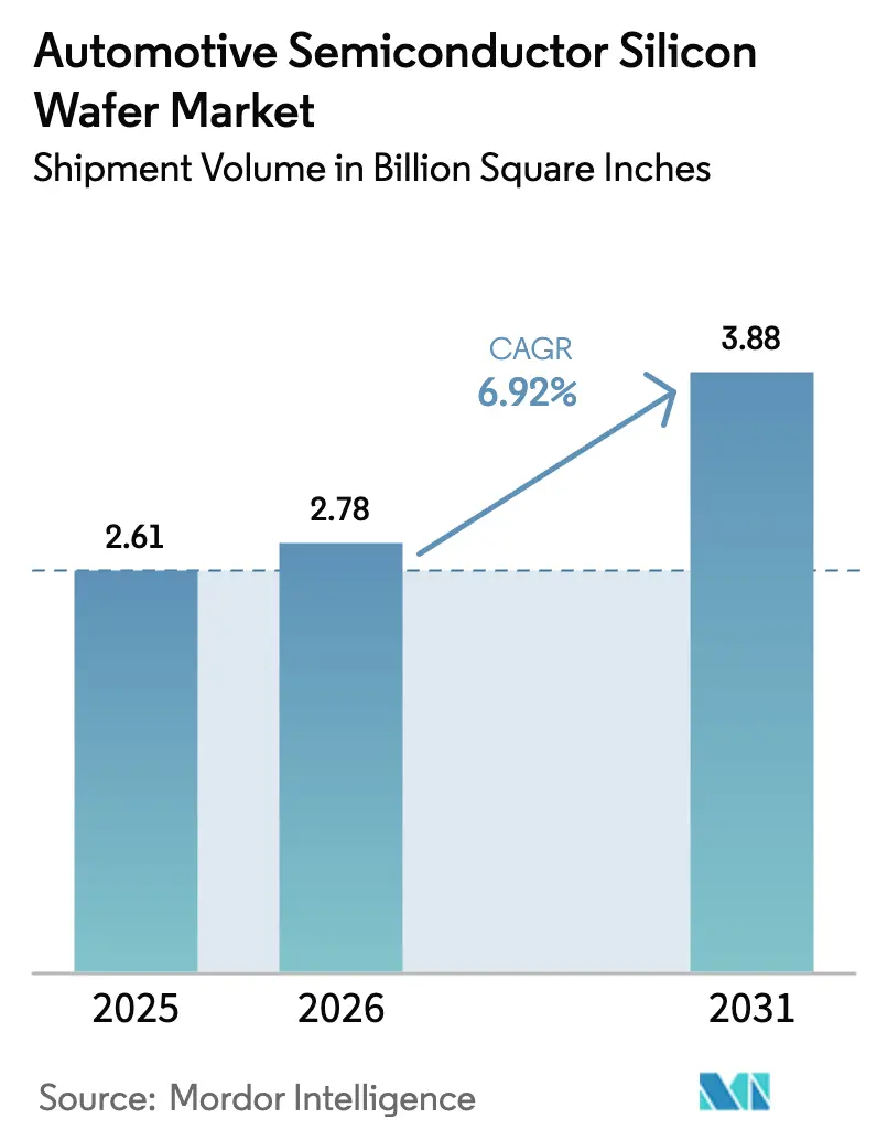
| Market Volume (2026) | 2.78 Billion Square Inches |
| Market Volume (2031) | 3.88 Billion Square Inches |
| Growth Rate (2026 - 2031) | 6.92% CAGR |
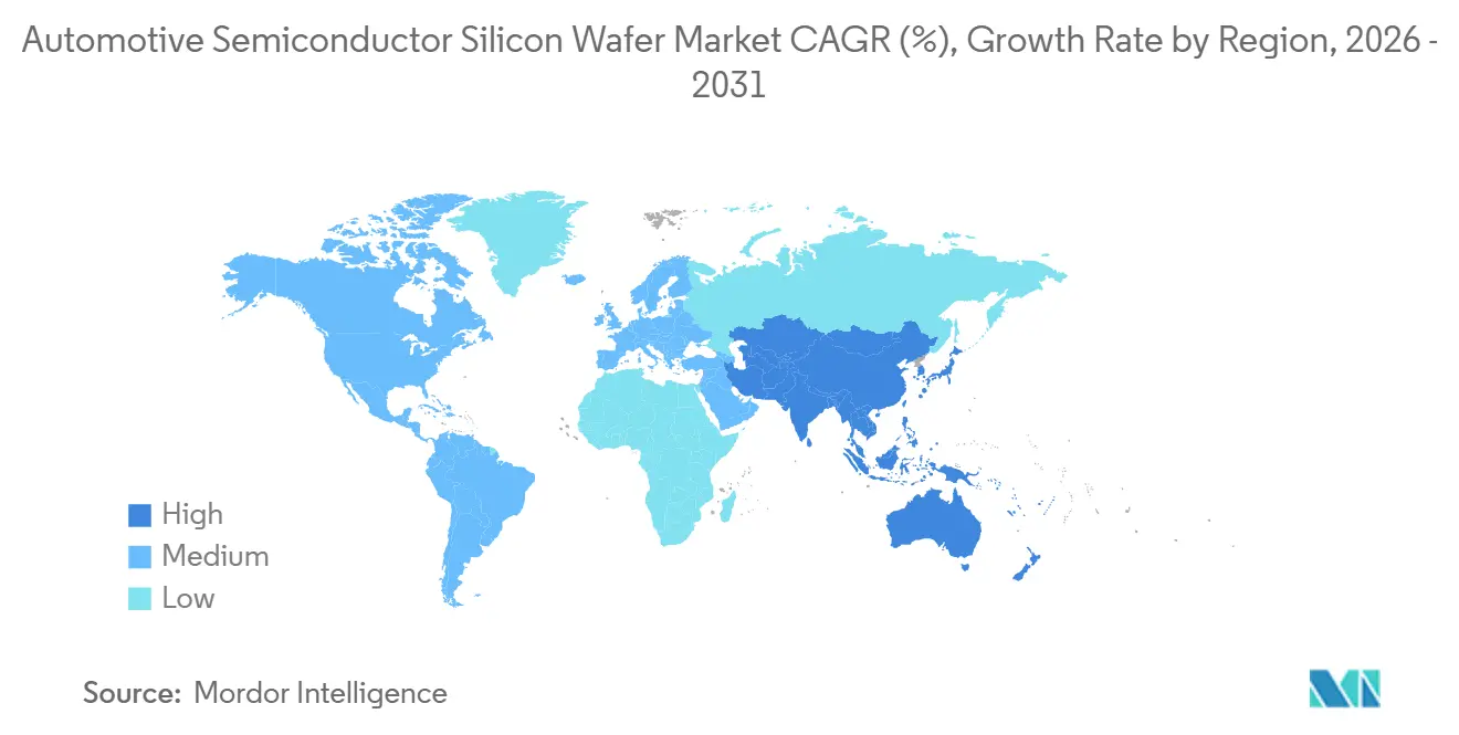
| Fastest Growing Market | Asia Pacific |
| Largest Market | Asia Pacific |
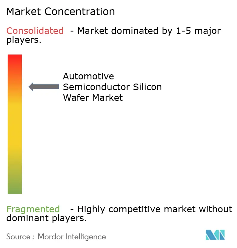
| Market Concentration | High |
Major Players *Disclaimer: Major Players sorted in no particular order Image © Mordor Intelligence. Reuse requires attribution under CC BY 4.0. | |
Automotive Semiconductor Silicon Wafer Market Analysis by Mordor Intelligence
The automotive semiconductor silicon wafer market size is expected to increase from 2.61 Billion Square Inches in 2025 to 2.78 billion Square Inches in 2026 and reach 3.88 Billion Square Inches by 2031, growing at a CAGR of 6.92% over 2026-2031. The expansion is powered by the rapid electrification of passenger vehicles, the migration to 800-volt battery packs, and the rise of software-defined vehicle compute domains. Wide-bandgap SiC epitaxial wafers on 200 mm substrates are absorbing much of the incremental volume, even as prime-polished silicon continues to ship the most pieces. Policy incentives in the United States, Europe, South Korea, and India are shortening fab paybacks, while ongoing substrate shortages and long automotive-grade qualification cycles moderate near-term output. Competitive moves toward vertical integration and 300 mm migration are reshaping cost curves and will decide the future trajectory of the automotive semiconductor silicon wafer market.
Key Report Takeaways
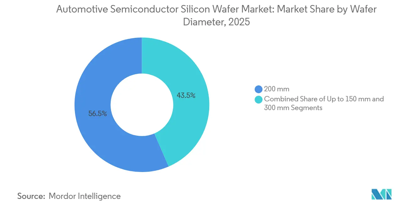
- By wafer diameter, 200 mm substrates led with 56.48% of automotive semiconductor silicon wafer market share in 2025, while 300 mm is projected to record the fastest 7.45% CAGR to 2031.
- By device type, discrete and power devices accounted for a 28.73% share of the automotive semiconductor silicon wafer market size in 2025 and are forecast to expand at a 7.38% CAGR through 2031.
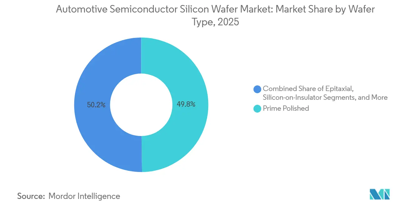
- By wafer type, prime polished wafers held 49.81% of the automotive semiconductor silicon wafer market share in 2025, whereas specialty silicon is advancing at a 7.78% CAGR to 2031.
- By geography, Asia-Pacific commanded 84.19% of automotive semiconductor silicon wafer market share in 2025 and is forecast to grow at 7.59% CAGR through 2031.
Note: Market size and forecast figures in this report are generated using Mordor Intelligence’s proprietary estimation framework, updated with the latest available data and insights as of January 2026.
Global Automotive Semiconductor Silicon Wafer Market Trends and Insights
Drivers Impact Analysis*
| Driver | (~) % Impact on CAGR Forecast | Geographic Relevance | Impact Timeline |
|---|---|---|---|
| Rising EV Penetration and Shift Toward 800V Vehicle Platforms | +2.1% | Global, with APAC and Europe leading adoption | Medium term (2-4 years) |
| Rapid Build-Out of 800V Charging Infrastructure | +1.3% | Europe, China, North America urban corridors | Medium term (2-4 years) |
| High-Temperature, High-Frequency Performance Advantages Over Si | +1.0% | Global, concentrated in EV traction and OBC applications | Long term (≥ 4 years) |
| Government Incentives for Wide-Band-Gap Fabs | +0.9% | North America, Europe, South Korea, India | Short term (≤ 2 years) |
| Emergence of Vertically-Integrated SiC Supply Chains in China | +0.7% | China, with spillover to Southeast Asia | Medium term (2-4 years) |
| Novel 200 mm Bulk-Growth Breakthroughs Lowering Defect Density | +0.5% | Global, led by Japan and US R&D centers | Long term (≥ 4 years) |
| Source: Mordor Intelligence | |||
Rising EV Penetration And Shift Toward 800V Vehicle Platforms
Electric models built on 800-volt packs need SiC MOSFETs rated at 1,200 V, which in turn require 200 mm epitaxial wafers with extremely low basal-plane dislocation densities. Launches such as Hyundai’s Ioniq 5 and Kia’s EV6 have triggered similar roadmaps from Porsche, Audi, and General Motors for model-year 2026 designs.[1]Hyundai Motor, “Ioniq 5 Specifications,” hyundai.com Capacity additions at Infineon’s Kulim facility and long-term wafer supply agreements signed by STMicroelectronics underscore the race to lock in material ahead of volume hikes. The structural pull tightens lead times beyond 12 months and underscores the importance of secure substrate access.
Rapid Build-Out Of 800V Charging Infrastructure
Public and private spending on ultra-fast charging surpassed USD 12 billion in 2025, and Europe’s AFIR rule mandates 400 kW chargers every 60 km on core corridors by 2027.[2]European Commission, “Alternative Fuels Infrastructure Regulation,” ec.europa.eu Each 800 V on-board charger integrates six to eight SiC MOSFETs grown on 150 mm- to 200-mm wafers, so faster charger rollouts translate directly into increased wafer demand. Chinese deployments already account for more than 60% of global 800 V posts, reinforcing Asia-Pacific’s dominance. Soitec’s Power-SOI substrates are winning gate-driver sockets where PCB area is tight. Because OBC design cycles lag infrastructure by roughly 18 months, the full volume effect will surface between 2027 and 2028.
High-Temperature, High-Frequency Performance Advantages Over Si
SiC devices withstand junction temperatures near 200 °C and switch at frequencies above 100 kHz, enabling automakers to shrink heatsinks by up to 40% and boost drive-cycle efficiency. Tesla’s 2024 Model 3 inverter switch yielded an efficiency lift equivalent to 15 miles of extra range per charge. The inherent high-frequency capability also reduces the need for passive components, a key benefit as battery voltages move toward 800 V and beyond. Complementary GaN-on-Si devices demonstrated by Soitec and Nanyang Technological University in 2026 show power-added efficiency above 50% at FR3, hinting at future mid-voltage adoption. Penetration remains below 20% of EV shipments, so upside extends well past 2030.
Government Incentives For Wide-Band-Gap Fabs
The US CHIPS Act granted GlobalWafers USD 4 billion to erect a 300 mm plant in Texas, while the EU’s IPCEI-ME/CT program supplied EUR 103 million (USD 110 million) to GlobalWafers’ Novara site. South Korea’s AI Era K-Semiconductor Vision commits the equivalent of USD 525 billion through 2047 and earmarks funds for 8-inch SiC demonstrators in Busan. India’s 50% cap-ex incentive is backing its first commercial SiC fab targeting 60,000 wafers per year. These grants shorten paybacks to six-to-eight years, clearing projects that private investors once judged marginal.
Restraints Impact Analysis*
| Restraint | (~) % Impact on CAGR Forecast | Geographic Relevance | Impact Timeline |
|---|---|---|---|
| Limited Availability of 200 mm Substrates | -1.2% | Global, most acute in North America and Europe | Short term (≤ 2 years) |
| Packaging-Induced Thermo-Mechanical Stress | -0.6% | Global, concentrated in high-power automotive modules | Medium term (2-4 years) |
| Capital-Intensive Crystal-Growth Equipment | -0.5% | Global, affecting new entrants and capacity expansions | Long term (≥ 4 years) |
| Recycling Challenges for SiC Kerf Waste | -0.2% | APAC and Europe, driven by ESG mandates | Long term (≥ 4 years) |
| Source: Mordor Intelligence | |||
Limited Availability Of 200 mm Substrates
Global capacity reached only 1.2 million 200 mm SiC wafers in 2025, yet automotive demand will surpass 2 million units before 2028.[3]Resonac Holdings, “SiC Epitaxy Strategy,” resonac.com Each PVT reactor costs up to USD 8 million and needs 18-24 months to qualify, delaying meaningful relief. Wolfspeed’s Siler City expansion runs through 2027, while European and North American OEMs still rely heavily on Asian imports. The shortage forces dual-sourcing and stretches design cycles, trimming 1.2 percentage points off the sector CAGR in the near term.
Packaging-Induced Thermo-Mechanical Stress
SiC’s 4.2 ppm °C-1 thermal expansion departs sharply from copper’s 17 ppm °C-1, generating shear stress that cracks die attach under automotive thermal cycling. Tier-1 suppliers report early field failures in 800 V inverter modules, prompting transitions to transient liquid phase bonding and low-CTE gels that add nearly USD 1 per module. Automotive qualification for double-sided cooling and embedded wafer-level BGA formats will take two to three years, during which yields stay below legacy IGBT benchmarks.
*Our forecasts treat driver/restraint impacts as directional, not additive. The impact forecasts reflect baseline growth, mix effects, and variable interactions.
Segment Analysis
By Wafer Diameter: Cost Pressure Fuels 300 mm Adoption
The 200 mm tranche held 56.48% automotive semiconductor silicon wafer market share in 2025 and remains indispensable for SiC power discretes, gate drivers, and PMICs. Mature-node lines already depreciated keep operating margins attractive, and the die sizes of traction MOSFETs fit 200 mm economics well. However, 300 mm capacity is climbing at a 7.45% CAGR because Texas Instruments, TSMC, and GlobalWafers are shifting MCUs and mixed-signal ICs onto larger wafers, driving 20%-plus cost reductions per die. Wolfspeed’s 300 mm SiC samples delivered sub-1 cm-2 defect densities, proving technical feasibility and pointing toward high-volume power‐device supply after 2028.
The automotive semiconductor silicon wafer market is likely to bifurcate, 300 mm will dominate compute and mixed-signal content once qualification barriers fall, while 200 mm persists in SiC until crystal growth catches up. Up-to-150 mm formats continue sliding as legacy fabs retire, although they retain pockets of demand for thyristors and custom analog. Soitec is migrating Power-SOI to 300 mm to meet demand for battery management, highlighting the need for tighter cost structures in electrification programs.


By Semiconductor Device Type: Power Discretes Outperform
Discrete and power devices accounted for 28.73% of the automotive semiconductor silicon wafer market size in 2025, with a projected 7.38% CAGR that outpaces logic and memory. Every EV traction inverter uses hundreds of MOSFET and diode chips, multiplying wafer needs even as die scale shrinks. Logic devices are consolidating into advanced nodes on 300 mm wafers, and embedded flash integration is trimming standalone memory consumption. Analog IC demand grows steadily as LiDAR, radar, and camera proliferation proliferate, though the area per device remains small.
Optoelectronics, sensors, and MEMS add incremental wafer pull, especially as LiDAR transmitter-receiver pairs rely on high-resistivity silicon or III-V wafers. STMicroelectronics’ 2026 takeover of a MEMS business places more sensor fabrication under the same roof as automotive MCUs, easing module-level pairing. The automotive semiconductor silicon wafer market share of power discretes will therefore keep climbing, reaffirming the power-conversion-centric nature of EV platforms.
By Wafer Type: Specialty Silicon Accelerates
Prime polished wafers retained 49.81% of the automotive semiconductor silicon wafer market share in 2025, yet specialty silicon is the fastest climber, with a 7.78% CAGR to 2031. High-resistivity substrates reduce RF losses for 5G V2X chips, and Power-SOI enables integrating 48 V and 200 V blocks on a single die, shrinking board area. Soitec and CEA-Leti demonstrated FD-SOI’s resilience to fault injection, aligning with ISO 26262 and ISO/SAE 21434 mandates.
Epitaxial silicon hovers near one-quarter of shipments because every high-voltage MOSFET and IGBT demands carefully doped drift regions. The automotive semiconductor silicon wafer market for SOI is growing as zonal controllers and battery monitors shift to secure substrates. Specialty silicon’s momentum thus stems from both electrification and cybersecurity requirements.
Geography Analysis
Asia-Pacific held 84.19% automotive semiconductor silicon wafer market share in 2025 and is expanding at 7.59% CAGR. Taiwan accounts for a considerable share of sub-6 nm capacity and more than 40% of mature-node automotive wafer starts, while China continues to integrate SiC crystal growth, epitaxy, and device fabs. South Korea’s 700 trillion KRW (USD 525 billion) strategy adds 10 new facilities and compound-semiconductor lines, reinforcing regional depth. Japan’s substrate majors, including Shin-Etsu and SUMCO, anchor 300 mm prime polished and SiC epitaxial supply, and India’s state-backed 12-inch line will bring 50,000 wafers per month online in 2026.
North America controlled a small share of shipments in 2025, but CHIPS Act incentives fund GlobalWafers’ 300 mm plant and Wolfspeed’s SiC megafab, together adding more than one million 200 mm-equivalent wafers annually by 2028. The localization push, however, still leaves many modules reliant on Asian substrates, as U.S. light-vehicle output surpasses 15 million units yearly. Europe holds a considerable share and benefits from IPCEI-ME/CT funding for capacity at Infineon, STMicroelectronics, and GlobalWafers, yet imports cover over 70% of prime polished demand.
South America plus Middle East and Africa together remain low due to limited ecosystem depth and capital barriers. To mitigate supply-chain risk, automakers now co-qualify multiple geographic sources even though the 18-to-24-month automotive-grade cycle delays meaningful diversification until late 2027. Inventory corrections that began in late-2024 appear to have bottomed by early-2026, and wafer call-offs are rebounding under new long-term supply agreements.

Competitive Landscape
The five largest prime polished suppliers-Shin-Etsu, SUMCO, Siltronic, GlobalWafers, and SK Siltron-control roughly more than half of global capacity, giving the automotive semiconductor silicon wafer market a moderately concentrated profile. Each is scaling 300 mm lines near major auto hubs to qualify for regional subsidies and to provide lower-carbon supply chains. In SiC, Wolfspeed, Coherent, SICC, and Resonac compete with vertically integrated IDMs such as Infineon, STMicroelectronics, and ON Semiconductor that are building captive substrate operations to secure volumes and protect margins.
Strategic thrusts cluster around three themes. First is vertical integration into specialty wafers that carry gross margins exceeding 40%, double those of commodity silicon. Second is geographic spread to satisfy subsidy rules and hedge geopolitical friction. Third is joint development with Tier-1s to tune wafer specs, cut cycle times, and lock in share. Technology edge matters, Soitec’s Smart Cut process delivers sub-100 nm uniformity in buried oxide, and Sumitomo Electric’s sub-0.1 cm-2 SiC dislocation metrics directly improve device yields.
White-space growth lies in 300 mm SiC substrates, sensor-grade silicon for LiDAR, and reclaim services for SiC kerf waste that today lands in landfill. Lesser-known players such as Okmetic, Wafer Works, and Topsil fill bespoke high-mix orders where incumbent minimums are prohibitive. Capital intensity of crystal growth remains a natural moat, PVT reactors cost up to USD 8 million and run for 200 hours per boule, reinforcing the advantage of deep-pocketed incumbents.
Automotive Semiconductor Silicon Wafer Industry Leaders
Shin-Etsu Chemical Co., Ltd.
SUMCO Corporation
GlobalWafers Co., Ltd.
Siltronic AG
SK Siltron Co., Ltd.
- *Disclaimer: Major Players sorted in no particular order

Recent Industry Developments
- February 2026: Soitec and Nanyang Technological University announced GaN-on-Si devices exceeding 50% power-added efficiency at FR3, supporting future automotive RF.
- February 2026: STMicroelectronics closed the acquisition of NXP’s MEMS business, integrating sensor production with MCU and power lines.
- February 2026: Soitec issued Q3 FY-2026 results showing sequential growth and guiding for a 20% Q4 increase under long-term automotive Power-SOI deals.
- December 2025: South Korea unveiled the AI Era K-Semiconductor Vision, allocating USD 525 billion through 2047 to compound-semiconductor and advanced-packaging clusters.


Global Automotive Semiconductor Silicon Wafer Market Report Scope
The Automotive Semiconductor Silicon Wafer Market Report is Segmented by Wafer Diameter (Up to 150 mm, 200 mm, and 300 mm), Semiconductor Device Type (Logic, Memory, Analog, Discrete, and Other Types), Wafer Type (Prime Polished, Epitaxial, SOI, and Specialty Silicon), and Geography (North America, Europe, Asia-Pacific, South America, Middle East and Africa). The Market Forecasts are Provided in Terms of Volume (Square Inches).
| Up to 150 mm |
| 200 mm |
| 300 mm |
| Logic |
| Memory |
| Analog |
| Discrete |
| Other Semiconductor Device Types |
| Prime Polished |
| Epitaxial |
| Silicon-on-Insulator (SOI) |
| Specialty Silicon (High-Resistivity, Power, Sensor-Grade) |
| North America | United States |
| Canada | |
| Mexico | |
| Europe | Germany |
| United Kingdom | |
| France | |
| Rest of Europe | |
| Asia-Pacific | China |
| Japan | |
| India | |
| South Korea | |
| Taiwan | |
| Rest of Asia-Pacific | |
| South America | |
| Middle East and Africa |
| By Wafer Diameter | Up to 150 mm | |
| 200 mm | ||
| 300 mm | ||
| By Semiconductor Device Type | Logic | |
| Memory | ||
| Analog | ||
| Discrete | ||
| Other Semiconductor Device Types | ||
| By Wafer Type | Prime Polished | |
| Epitaxial | ||
| Silicon-on-Insulator (SOI) | ||
| Specialty Silicon (High-Resistivity, Power, Sensor-Grade) | ||
| By Geography | North America | United States |
| Canada | ||
| Mexico | ||
| Europe | Germany | |
| United Kingdom | ||
| France | ||
| Rest of Europe | ||
| Asia-Pacific | China | |
| Japan | ||
| India | ||
| South Korea | ||
| Taiwan | ||
| Rest of Asia-Pacific | ||
| South America | ||
| Middle East and Africa | ||


Key Questions Answered in the Report
How fast will demand for automotive SiC wafers grow through 2031?
Unit volume tied to electric traction inverters pushes SiC wafer demand at a 7%-plus CAGR, faster than total automotive wafer consumption.
Which wafer diameter will dominate automotive microcontrollers by 2030?
Most newly released MCUs will migrate to 300 mm lines to lower die cost and improve availability.
Why are 200 mm SiC substrates still critical despite 300 mm pilots?
200 mm delivers proven crystal growth yields and supports today’s EV ramps, while 300 mm requires several more years of qualification.
What drives the shift toward specialty silicon in vehicles?
Functional safety and cybersecurity mandates favor FD-SOI and high-resistivity substrates, while ADAS sensors need low-loss RF silicon.
Page last updated on:


