Market Overview
| Study Period | 2019 - 2030 |
| Market Size (2025) | USD 30.65 Billion |
| Market Size (2030) | USD 45.54 Billion |
| Growth Rate (2025 - 2030) | 8.24% CAGR |
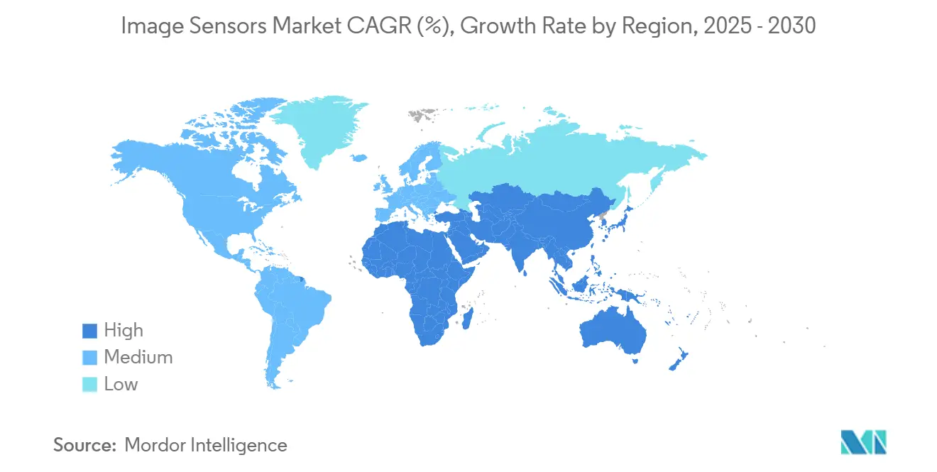
| Fastest Growing Market | Asia Pacific |
| Largest Market | North America |
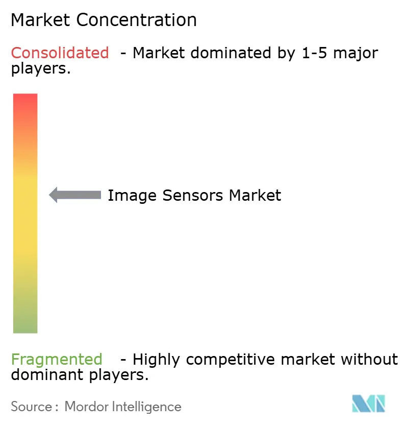
| Market Concentration | Medium |
Major Players
*Disclaimer: Major Players sorted in no particular order Image © Mordor Intelligence. Reuse requires attribution under CC BY 4.0. |
|
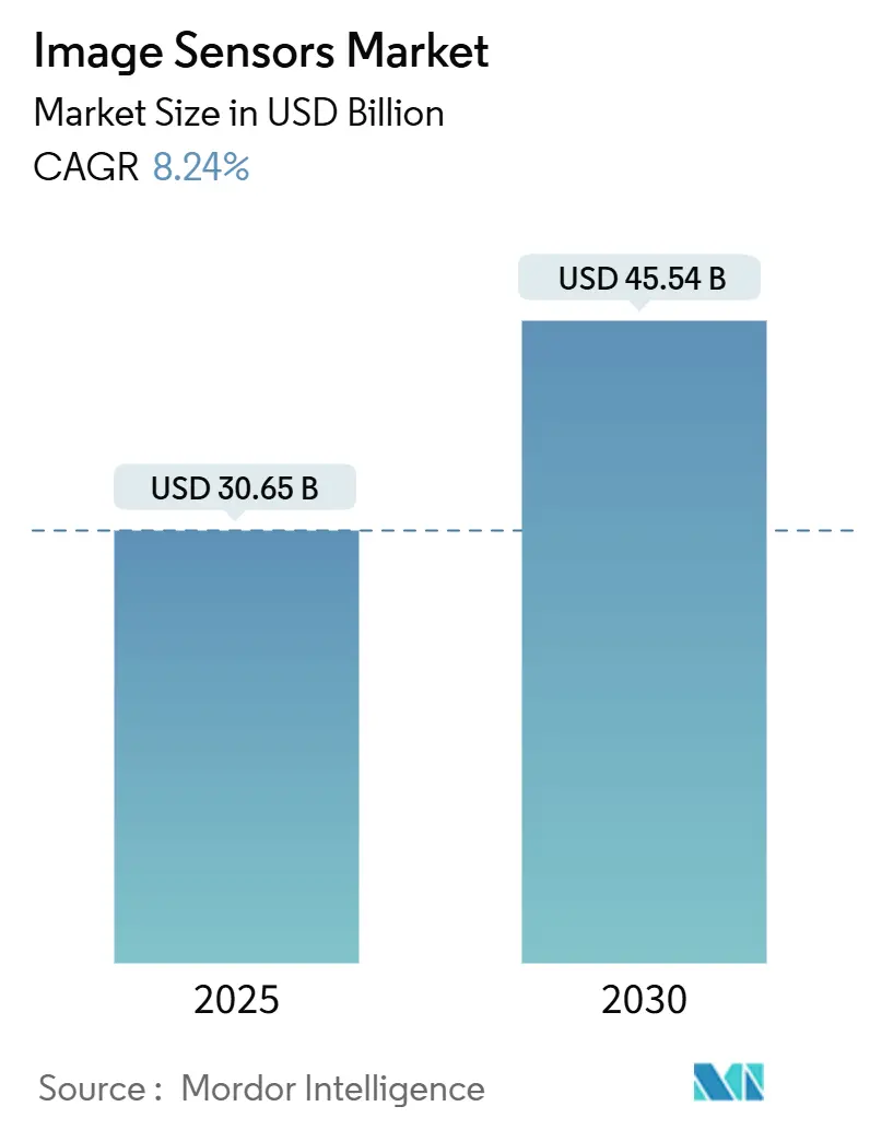
Image Sensors Market Analysis by Mordor Intelligence
The image sensor market reached USD 30.65 billion in 2025 and is projected to expand to USD 45.54 billion by 2030, translating to an 8.24% CAGR over the forecast period. Growth reflects a confluence of automotive safety mandates, sophisticated multi-camera smartphones, and industrial automation needs that are reshaping semiconductor demand. Vehicle makers are equipping an average of 8 cameras per car in 2025 and plan to add 12 cameras by 2028, accelerating sensor volumes and ASP expansion. CMOS devices capture 93% of 2024 unit shipments because of low-power on-chip processing, while stacked back-side-illuminated (BSI) designs, scaling at a 55% CAGR to 2030, unlock higher dynamic range and AI computation at the edge. The 4–12 MP resolution bracket dominates with 32% revenue because it balances image quality and cost for mainstream consumer and industrial use. Competitive intensity is rising as Sony, Samsung, OmniVision and onsemi defend share against new entrants amid geopolitical export controls, 300 mm wafer scarcity, and thermal-noise barriers that slow sub-micron pixel shrink.
Key Report Takeaways
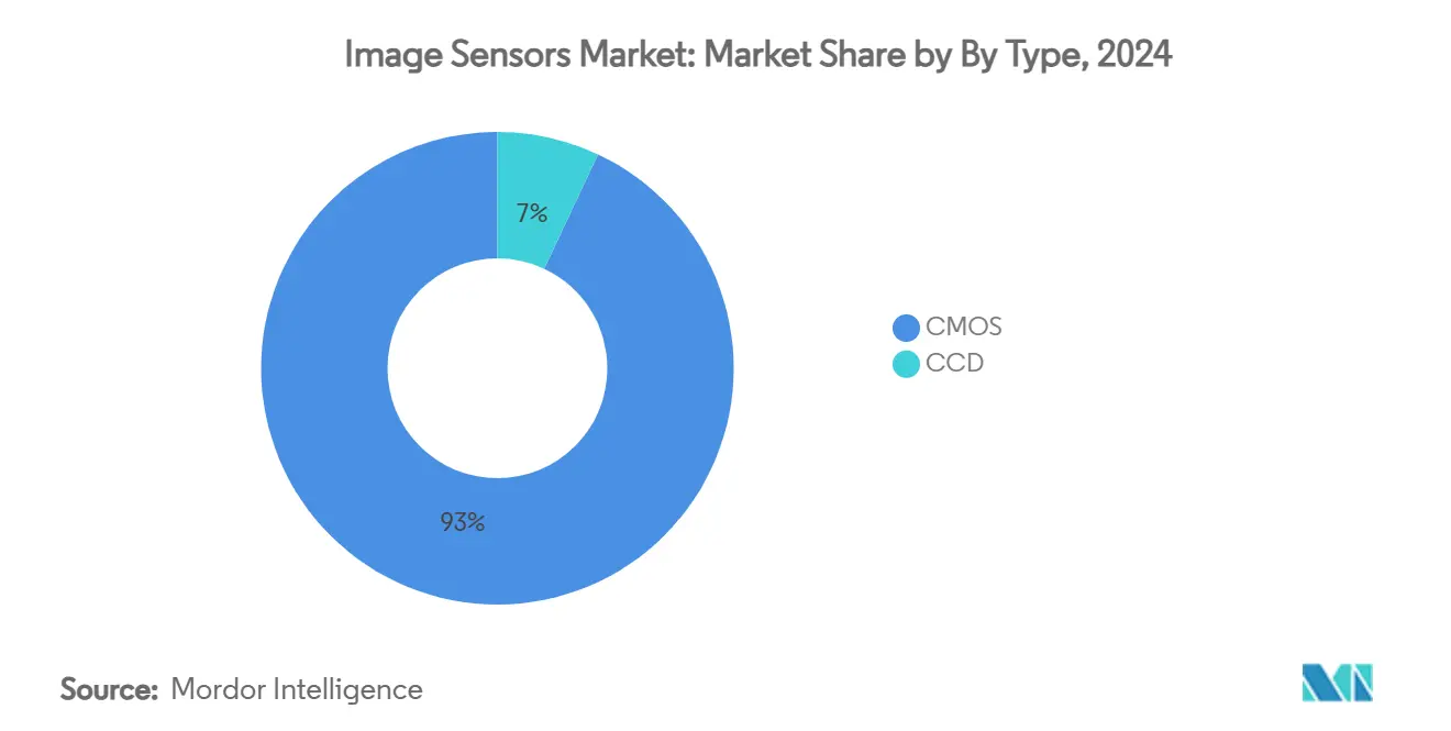
- By sensor type, CMOS commanded 93% of the image sensor market share in 2024 while CCD retained niche scientific uses; stacked CMOS is forecast to grow at 55% CAGR to 2030.
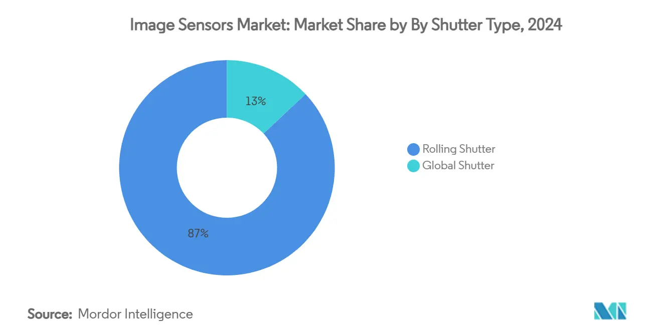
- By shutter, rolling variants held 87% of the image sensor market share in 2024; global shutter revenue is expected to expand at 18.6% CAGR through 2030.
- By resolution, the 4–12 MP band accounted for 32% of the image sensor market size in 2024 and will grow at 7.4% CAGR to 2030.
- By end-user, consumer electronics provided 27% revenue in 2024; automotive is the fastest-growing end-user segment with an 11.2% CAGR to 2030.
- By geography, Asia-Pacific generated the largest image sensor market size in 2025, while North America is set to post the highest 9.1% CAGR to 2030.
Global Image Sensors Market Trends and Insights
Drivers Impact Analysis
| DRIVER | (~) % IMPACT ON CAGR FORECAST | GEOGRAPHIC RELEVANCE | IMPACT TIMELINE |
|---|---|---|---|
| Automotive-grade image sensors fueling ADAS & autonomous deployment | +2.1% | Global (North America, Europe, Japan) | Medium term (2–4 years) |
| Penetration of multi-camera smartphones with high-resolution CMOS BSI sensors | +1.8% | APAC core, spill-over global | Short term (≤ 2 years) |
| Growing adoption of SWIR/NIR sensors in precision agriculture & industrial inspection | +1.2% | North America & EU, expanding to APAC | Long term (≥ 4 years) |
| Edge-AI-enabled vision modules accelerating IoT & smart city projects | +0.9% | Europe core, expanding to North America & APAC | Medium term (2–4 years) |
| Rising demand for global shutter sensors in AR/VR wearables | +0.7% | Global, early in North America & Asia | Medium term (2–4 years) |
| Government safety mandates for ADAS cameras | +1.3% | North America & Japan | Short term (≤ 2 years) |
Source: Mordor Intelligence
Understand The Key Trends Shaping This Market
Download PDF
Automotive-grade Image Sensors Fueling ADAS & Autonomous Deployment
Automotive safety regulation is shifting cameras from premium options to mandated equipment, transforming the image sensor market. onsemi’s Hyperlux AR0823AT won Subaru’s next-gen EyeSight stereo-camera slot, meeting ASIL-C targets for autonomous decision making. Canon’s prototype 410 MP sensor processes 3,280 MP/s, showing that modern sensors are computational platforms, not passive imagers. Sony projects a 6.68-fold jump in car camera nodes between 2019 and 2030, highlighting sustained OEM pull for high-dynamic-range, low-latency parts. HDR, LED-flicker mitigation and functional-safety IP now come standard, positioning automotive imagers as critical safety infrastructure.[1]onsemi, “Hyperlux Sensors Selected for Subaru EyeSight,” onsemi.com
Penetration of Multi-Camera Smartphones with High-Resolution CMOS BSI Sensors in Asia
Asia’s handset ecosystem keeps driving pixel-architecture breakthroughs. Samsung converted its Hwaseong line to stacked CIS fabrication starting 2025, chasing premium iPhone design wins. Its 3-layer sensor splits photodiode, transfer and logic strata, boosting dynamic range while shrinking footprint. OmniVision’s OV50X delivers 110 dB single-exposure HDR with 1.6 µm pixels, proving Asian suppliers now lead in low-light computational imaging. The shift from megapixel race to image quality underscores a mature smartphone cycle where advanced BSI and AI ISP integration differentiate user experience.
Growing Adoption of SWIR/NIR Sensors in Precision Agriculture & Industrial Inspection
Short-wave infrared (SWIR) once cost-prohibitive, is pivoting to commercial scale. STMicroelectronics introduced a quantum-dot SWIR array with 1.62 µm pitch and 60% QE, aiming for single-dollar ASPs. Lower materials cost unlocks moisture, crop-stress and polymer-sorting use cases. Quality Magazine forecasts a 28% CAGR from USD 89 million in 2022 to USD 395 million by 2028 for SWIR imaging. Industrial inspection lines adopt SWIR to detect contaminants invisible to visible light, extending factory automation ROI.
Edge-AI-Enabled Vision Modules Accelerating IoT & Smart City Projects
Strict European privacy laws encourage on-sensor intelligence to limit cloud transfer. Research on smart pixels shows in-pixel AI can reject 54–75% redundant data at 6 µW per pixel, slashing bandwidth while conserving energy. ams OSRAM secured EUR 227 million Chips Act funding to expand Austrian fabs building edge-AI optical sensors for smart streetlights and traffic nodes. Coupling microLED display drivers with sensing lets urban devices merge visualization and data capture, streamlining maintenance and cost.
Restraints Impact Analysis
| RESTRAINTS | (~) % IMPACT ON CAGR FORECAST | GEOGRAPHIC RELEVANCE | IMPACT TIMELINE |
|---|---|---|---|
| Supply-chain concentration in 300 mm wafer fabs | -1.4% | Global, acute in APAC | Short term (≤ 2 years) |
| Thermal noise & power limits in sub-micron pixel shrink | -0.8% | Global | Long term (≥ 4 years) |
| Export controls on advanced imaging chips | -1.1% | China core, ripple global | Medium term (2–4 years) |
| High integration cost of SWIR sensors | -0.6% | Global, price-sensitive markets | Medium term (2–4 years) |
Source: Mordor Intelligence
Supply-Chain Concentration in 300 mm Wafer Fabs Creating Price Volatility
SEMI records 30 million wafers-per-month capacity in 2024, yet production clusters around a handful of Asian foundries, amplifying shortages during demand spikes. Image sensor lines now compete with high-margin AI accelerators for the same 300 mm tools, lifting die prices and lengthening lead times. McKinsey observes that 60% of specialty chemicals needed for lithography lack local US supply, adding upstream risk. Until Arizona and European fabs reach volume after 2026, price swings will compress margins across the image sensor market.
Thermal Noise & Power Limits in Sub-Micron Pixel Shrink Challenging Further Resolution Gains
When pixel pitch drops below 1 µm, thermal noise erodes signal-to-noise ratio, forcing costly circuit tricks such as Skipper-in-CMOS readout that achieves 0.15 e- rms yet raises complexity. SPIE analyses show tighter pitches demand optics with faster f-numbers, complicating module design. As power budgets tighten, vendors pivot to stacked BSI and on-sensor AI to boost effective resolution without endless pixel shrink.[2]SEMI, “Global Semiconductor Capacity Projected to Expand 6% in 2024,” semi.org
Segment Analysis
By Type: CMOS Dominance Drives Innovation
CMOS sensors owned 93% of unit shipments in 2024, underscoring their low-power logic integration and per-wafer economics. The image sensor market size for CMOS reached USD 28.7 billion in 2025, dwarfing CCD revenues. Column-parallel ADC and backside wiring lift frame rate while shrinking die area, letting vendors ship 5–7 billion parts yearly for phones alone. Scientific and medical instruments continue ordering CCDs for ultra-low dark current, yet fab investments trend to CMOS, ensuring its share rises. Samsung’s 3-layer stack demonstrates how separating photodiode, transfer and logic planes lifts quantum efficiency and reduces crosstalk, cementing CMOS leadership.
Second-generation stacked CIS improves redundancy and defect management, driving a projected 10.2% unit CAGR for CMOS through 2030. This momentum allows new entrants from China and India to license mature-node 65 nm flows and still launch competitive imagers for automotive surround-view. The image sensor market remains anchored on CMOS innovation as foundries add buried oxide isolation and hybrid bonding lines dedicated to photonics modules.[3]Annual Review of Vision Science, “Digital Image Sensor Evolution,” annualreviewofvisionscience.org
By Processing Technology: Stacked BSI Leads Innovation
Stacked BSI shipments are growing at 55% CAGR because vertical integration circumvents 2-D scaling limits. Separating photodiode and logic layers permits larger light-collection areas without enlarging die, yielding 1.5–2 EV sensitivity uplift. Canon’s 410 MP stacked full-frame sensor reads 3,280 MP/s via 40 parallel lanes, showing high-performance potential. Manufacturing yields have risen as wafer-to-wafer hybrid bonding moves from pilot to 24/7 production, cutting cost by 30% versus through-silicon-via stacking.
Within the image sensor market, stacked BSI is forecast to command USD 25.9 billion of image sensor market size by 2030, underpinned by smartphone and automotive ADAS volume ramps. Front-side and conventional BSI remain viable in low-tier devices where cost dominates, but premium makers now align roadmaps around multi-layer stacks that embed ISP blocks, SDRAM and AI accelerators under the pixel matrix, driving system-in-package convergence.
By Shutter Type: Rolling Dominates Despite Global Growth
Rolling shutter captured 87% revenue in 2024 because simpler sequenced readout keeps die area small and power lower. Page-based motion-blur correction in smartphones and drones makes rolling viable in most use cases. Conversely, global shutter is expanding 18.6% CAGR thanks to AR/VR, robotics and autonomous vehicles that cannot tolerate distortion. Meta’s patent details multi-mode sensors toggling between rolling and global readout to balance power and precision.
The image sensor market share for global shutter is expected to reach 19% by 2030 as high-speed machine-vision lines and head-mounted displays proliferate. New pixel architectures store charge under a shielding metal layer, permitting >120 dB HDR without rolling artifacts. Vendors such as Teledyne e2v pair global shutter with depth-mapping phase masks, converging 2-D, 3-D and NIR sensing in one die
By Spectrum: Visible RGB Leads with NIR Growth
Visible RGB remained the volume engine, generating 35% revenue as of 2024, yet demand for NIR and SWIR is outpacing. STMicroelectronics’ quantum-dot breakthrough positions SWIR to penetrate consumer appliances once cost dips below USD 2 per module. Agriculture, food sorting, and Li-metal battery inspection rely on NIR/SWIR penetration to reveal moisture or defect signatures invisible to visible light.
Hyperspectral projects in recycling plants combine 32-band chips into conveyor cameras that identify polymers or textiles, reflecting how the image sensor market is diversifying beyond RGB. X-ray and UV sensors continue in medical and semiconductor metrology niches, where regulatory and integration hurdles keep volume limited.
Geography Analysis
North America remains the largest regional buyer measured in revenue because ADAS regulations and defense procurements drive high-spec ASP. The United States finalized automatic emergency braking rules that implicitly require forward-facing cameras in all light vehicles from 2029, locking long-tail demand. Canada’s Tier-1 suppliers cluster around Ontario’s automotive corridor, and Mexico hosts module assembly for US OEMs. The region’s push for semiconductor sovereignty spurred TSMC’s USD 165 billion Arizona megafab, anticipated to supply mature-node CIS wafers post-2027.
Europe emphasizes privacy-first smart cities, funding edge-AI image sensors via the Chips Act. ams OSRAM’s EUR 588 million Austrian expansion will feed both automotive lidar and municipal traffic nodes. Germany and France enforce Euro-NCAP camera benchmarks that trickle to suppliers across the continent. Local regulations cap cloud storage of facial data, encouraging in-sensor encryption and on-device inference, cultivating a premium for secure image sensor market designs.
Asia-Pacific houses most wafer capacity and posts the fastest shipment growth. Japan’s Sony aims for 43% automotive CMOS share by 2026 on the back of Tier-1 alliances. South Korea’s Samsung is retooling Hwaseong for additional 200,000 wafers-per-month CIS output to backfill smartphone and AR/VR cameras. China increases remote-sensing demand for its Jilin-1 constellation yet faces US export controls on advanced 28 nm CIS nodes, prompting domestic foundries to accelerate mature-process investments. India emerges as a consumption-driven market for automotive dash-cams and low-cost phones, while Israel develops niche defense imagers in GaAs fabs, extending regional diversity.
Competitive Landscape
Sony leads the image sensor market through stacked BSI IP and automotive design-ins, holding 32% revenue in 2023 and targeting 43% by 2026. Samsung intensifies rivalry via 3-layer sensors aimed at iPhone contracts, leveraging foundry-logic alignment to shorten development loops. OmniVision competes on HDR and low-light performance with its OV50X, gaining traction in Chinese flagships.
Second-tier players such as onsemi specialize in automotive ASIL-compliant parts, while STMicroelectronics pushes cost-down SWIR modules ready for consumer IoT. Teledyne e2v extends into 3-D depth sensors after partnering with Airy3D, broadening industrial offerings. SK Hynix, struggling at 4% share, redirected wafer starts to high-bandwidth memory, signaling consolidation pressure among lagging competitors.
Strategic themes include vertical integration from wafer to module, hybrid wafer bonding to embed DRAM under pixels, and regionalizing fabs to navigate trade policy. Mature-node CIS fetches steady margins because of IP barriers and automotive qualification cycles, keeping the image sensor market moderately concentrated yet innovation-intensive.
Image Sensors Industry Leaders
-
Sony Group Corp.
-
Samsung Electronics Co., Ltd.
-
OmniVision Technologies, Inc.
-
STMicroelectronics N.V.
-
ON Semiconductor Corporation
- *Disclaimer: Major Players sorted in no particular order
Need More Details on Market Players and Competitors?
Download PDF
Recent Industry Developments
- January 2025: Canon developed a 410-megapixel CMOS sensor achieving the highest pixel count for a 35mm full-frame sensor, targeting surveillance, medical, and industrial applications with 24K resolution equivalent and 3,280 megapixels per second readout speed.
- Januray 2025: ams OSRAM received EU Commission approval for EUR 227 million investment grant to expand semiconductor manufacturing in Austria, with total investment reaching EUR 567 million by 2030 for next-generation optoelectronic sensors.
- January 2025: Samsung developed 3-layer stacked image sensors featuring separate photodiode, transfer, and logic layers to compete with Sony's exclusive iPhone sensor supply, targeting iPhone 18 production in 2026.
- November 2024: Hamamatsu Photonics acquired BAE Systems Imaging Solutions for undisclosed amount, rebranding it as Fairchild Imaging to strengthen opto-semiconductor segment and expand North American market presence.
Global Image Sensors Market Report Scope
The image sensor is a device that detects and conveys information used to make an image by converting the variable attenuation of the light waves into the signals that give the information.
The image sensors market is segmented by type (CMOS, CCD), end-user industry (consumer electronics, healthcare, industrial, security and surveillance, automotive & transportation, aerospace & defense), and geography (North America (United States, Canada), Europe (United Kingdom, Germany, France, Rest of Europe), Asia Pacific (China, India, Japan, Rest of Asia Pacific), Rest of the World). The market sizes and forecasts are provided in terms of value in (USD) for all the above segments.
| By Type | CMOS | ||
| CCD | |||
| By Processing Technology | Front-Side Illuminated (FSI) | ||
| Back-Side Illuminated (BSI) | |||
| Stacked BSI | |||
| By Shutter Type | Rolling Shutter | ||
| Global Shutter | |||
| By Spectrum | Visible (RGB) | ||
| Near-Infrared (NIR) | |||
| Short-Wave Infrared (SWIR) | |||
| X-ray / UV | |||
| By Resolution | Less than 1 MP | ||
| 1-3 MP | |||
| 4-12 MP | |||
| 13-24 MP | |||
| Greater than or Equal to 25 MP | |||
| By End-User Industry | Consumer Electronics | ||
| Automotive and Transportation | |||
| Industrial Automation and Robotics | |||
| Security and Surveillance | |||
| Healthcare and Life Sciences | |||
| Aerospace and Defense | |||
| Others (Smart City, Agriculture, Marine) | |||
| By Geography | North America | United States | |
| Canada | |||
| Mexico | |||
| Europe | United Kingdom | ||
| Germany | |||
| France | |||
| Italy | |||
| Rest of Europe | |||
| Asia-Pacific | China | ||
| Japan | |||
| India | |||
| South Korea | |||
| Rest of Asia-Pacific | |||
| Middle East | Israel | ||
| Saudi Arabia | |||
| United Arab Emirates | |||
| Turkey | |||
| Rest of Middle East | |||
| Africa | South Africa | ||
| Egypt | |||
| Rest of Africa | |||
| South America | Brazil | ||
| Argentina | |||
| Rest of South America | |||
By Type
| CMOS |
| CCD |
By Processing Technology
| Front-Side Illuminated (FSI) |
| Back-Side Illuminated (BSI) |
| Stacked BSI |
By Shutter Type
| Rolling Shutter |
| Global Shutter |
By Spectrum
| Visible (RGB) |
| Near-Infrared (NIR) |
| Short-Wave Infrared (SWIR) |
| X-ray / UV |
By Resolution
| Less than 1 MP |
| 1-3 MP |
| 4-12 MP |
| 13-24 MP |
| Greater than or Equal to 25 MP |
By End-User Industry
| Consumer Electronics |
| Automotive and Transportation |
| Industrial Automation and Robotics |
| Security and Surveillance |
| Healthcare and Life Sciences |
| Aerospace and Defense |
| Others (Smart City, Agriculture, Marine) |
By Geography
| North America | United States |
| Canada | |
| Mexico | |
| Europe | United Kingdom |
| Germany | |
| France | |
| Italy | |
| Rest of Europe | |
| Asia-Pacific | China |
| Japan | |
| India | |
| South Korea | |
| Rest of Asia-Pacific | |
| Middle East | Israel |
| Saudi Arabia | |
| United Arab Emirates | |
| Turkey | |
| Rest of Middle East | |
| Africa | South Africa |
| Egypt | |
| Rest of Africa | |
| South America | Brazil |
| Argentina | |
| Rest of South America |
Need A Different Region or Segment?
Customize Now
Key Questions Answered in the Report
What is the current size of the image sensor market?
The image sensor market stands at USD 30.65 billion in 2025 and is projected to reach USD 45.54 billion by 2030.
Which sensor type dominates the image sensor market?
CMOS technology dominates with 93% market share in 2024 thanks to integrated processing and lower power needs.
Why are stacked BSI sensors growing so fast?
Stacked BSI separates photodiodes and logic across layers, raising sensitivity and embedding AI, driving a 55% CAGR toward 2030.
How many cameras does an average car use today?
Vehicles use about 8 cameras in 2025 and are expected to integrate 12 by 2028 to support ADAS and autonomous functions.
What regional market is expanding quickest?
Asia-Pacific supplies most global volume, but North America posts the fastest 9.1% CAGR to 2030 due to safety regulations and defense investment.
What is the main supply-chain risk for image sensor producers?
Heavy reliance on a few 300 mm fabs causes price swings and allocation challenges when demand spikes for other semiconductors like AI accelerators.
Page last updated on: July 8, 2025

