
Asia-Pacific Semiconductor Manufacturing Equipment Market Size and Share
Market Overview
| Study Period | 2020 - 2031 |
|---|---|
| Forecast Data Period | 2026 - 2031 |
| Base Year Market Size (2025) | USD 92.14 Billion |
| Market Size (2026) | USD 101.35 Billion |
| Market Size (2031) | USD 181.02 Billion |
| Growth Rate (2026 - 2031) | 12.30 % |
| Market Concentration | Medium |
Major Players *Disclaimer: Major Players sorted in no particular order Image © Mordor Intelligence. Reuse requires attribution under CC BY 4.0. | |
Asia-Pacific Semiconductor Manufacturing Equipment Market Analysis by Mordor Intelligence
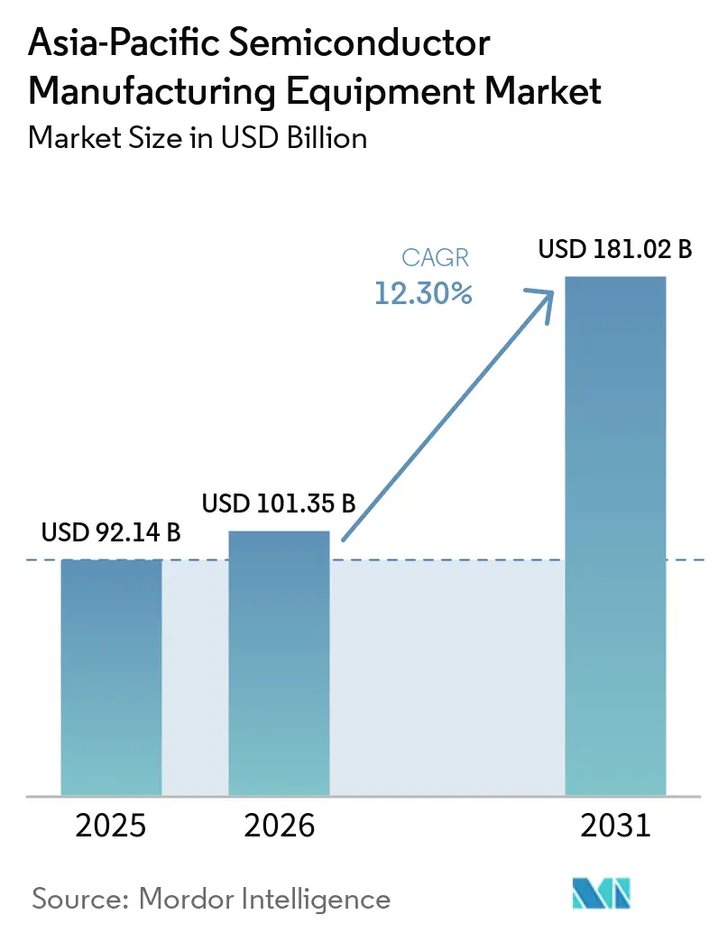
The Asia-Pacific Semiconductor Manufacturing Equipment Market size is expected to grow from USD 92.14 billion in 2025 to USD 101.35 billion in 2026 and is forecast to reach USD 181.02 billion by 2031 at 12.30% CAGR over 2026-2031.
The Asia-Pacific semiconductor manufacturing equipment market continues to attract sustained investment, led by China, Taiwan, South Korea, and Japan. Capacity expansions in advanced logic, memory, and advanced packaging are driving equipment demand across the region. The rapid adoption of AI-driven computing is increasing the number, complexity, and precision requirements of semiconductor manufacturing processes, leading to higher investments in lithography, deposition, etching, metrology, inspection, and packaging equipment for advanced logic, DRAM, NAND, and high-bandwidth memory (HBM) production. At the same time, government-supported semiconductor programs in countries such as India, Malaysia, Singapore, and Vietnam are expanding the regional manufacturing footprint by attracting investments in wafer fabrication, assembly, testing, and packaging facilities. Meanwhile, export controls and geopolitical tensions are reshaping supply chains and creating distinct technology ecosystems for leading-edge and mature-node semiconductor manufacturing, influencing equipment sourcing and localization strategies. As a result, large-scale fab investments increasingly shape the Asia-Pacific semiconductor manufacturing equipment market. Equipment suppliers must qualify advanced tools, localize manufacturing and service capabilities, support expanding installed equipment bases, and meet the evolving technical requirements of next-generation semiconductor production.
Key Report Takeaways
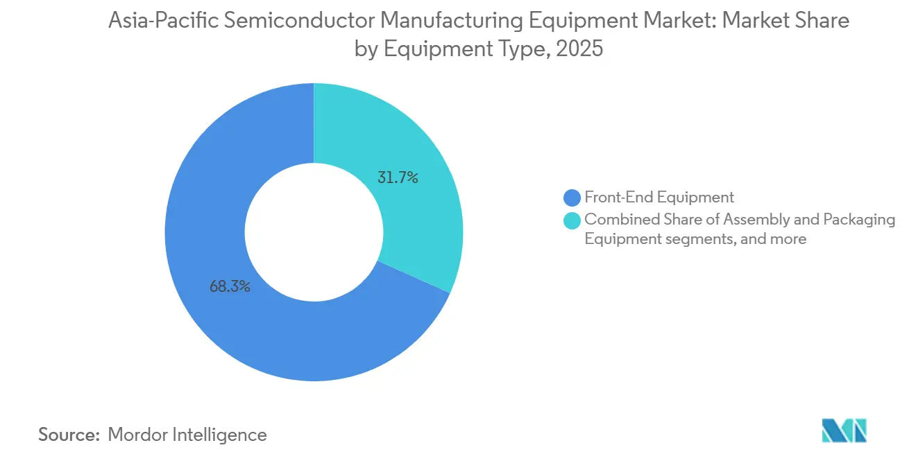
- By equipment type, wafer fab equipment/front-end equipment accounted for 68.30% of the Asia-Pacific semiconductor manufacturing equipment market share in 2025, while assembly and packaging equipment are projected to be the fastest-growing, with a 14.50% CAGR through 2031.
- By device type, logic and microcomponents accounted for 34.00% of the Asia-Pacific semiconductor manufacturing equipment market size in 2025, while the memory segment is projected to be the fastest-growing, with a 13.95% CAGR through 2031.
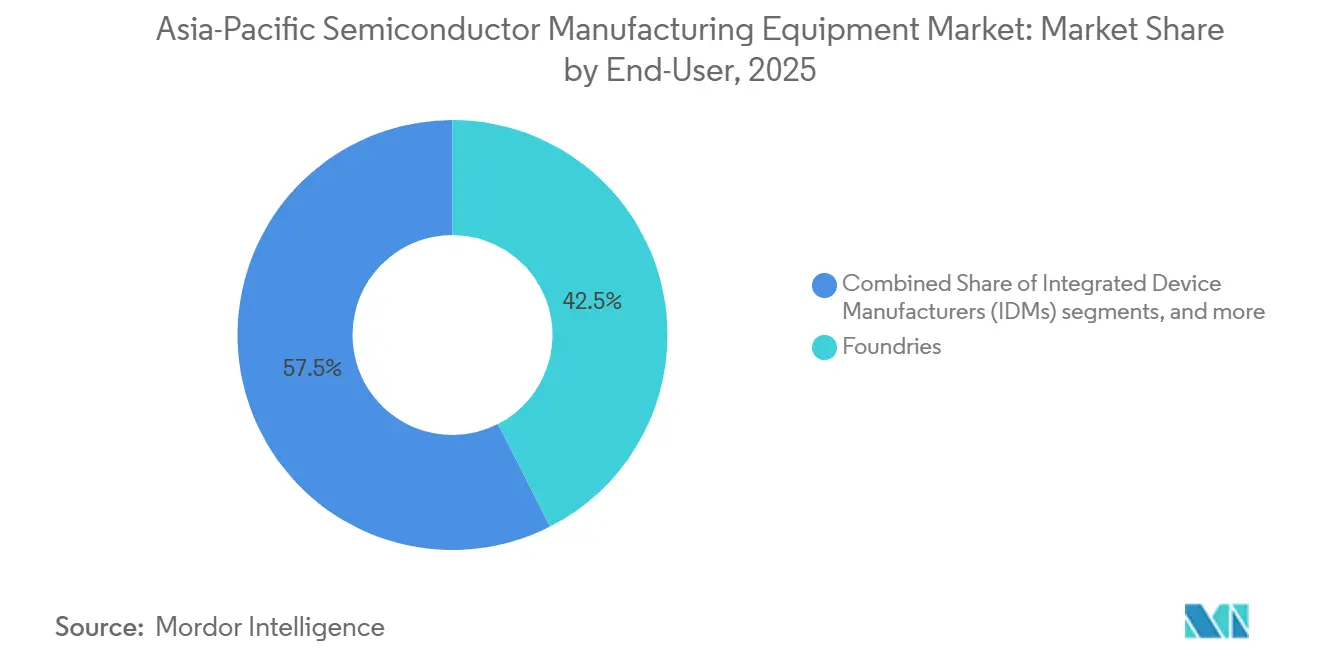
- By end user, the foundries segment accounted for 42.50% of the market in 2025 and is expected to remain the fastest-growing segment, with a 13.70% CAGR through 2031.
- By geography, China held the leading position, accounting for 38.70% of the market share in 2025 and is expected to remain the fastest-growing regional segment at a 13.30% CAGR through 2031.
Note: Market size and forecast figures in this report are generated using Mordor Intelligence’s proprietary estimation framework, updated with the latest available data and insights as of January 2026.
Asia-Pacific Semiconductor Manufacturing Equipment Market Trends and Insights
Drivers Impact Analysis*
| Driver | (~) % Impact on CAGR Forecast | Geographic Relevance | Impact Timeline | |
|---|---|---|---|---|
| AI, HPC, and HBM Capacity Expansion | +3.2% | Taiwan, South Korea, Asia-Pacific-wide spill-over | Short term (≤ 2 years) | |
| Advanced-Node Migration to GAA and 2nm-Class Production | +2.6% | Taiwan, South Korea, Japan | Medium term (2-4 years) | |
| Government-Led Semiconductor Localization and Fab Incentives | +2.0% | China, India, Japan, South Korea | Medium term (2-4 years) | |
| Advanced Packaging and Heterogeneous Integration | +1.6% | Taiwan, South Korea, Singapore, Asia-Pacific-wide | Medium term (2-4 years) | |
| China Equipment Localization and Mature-Node Capacity Build-Out | +1.2% | China, spill-over to the rest of Asia-Pacific | Short term (≤ 2 years) | |
| Equipment Demand from Power, Automotive, and Compound Semiconductors | +0.6% | China, Japan, South Korea | Long term (≥ 4 years) | |
| Source: Mordor Intelligence | ||||
AI, HPC, and HBM Capacity Expansion
AI and high-performance computing are raising equipment demand across Taiwan and South Korea, where advanced logic and HBM capacity programs are concentrated. SEMI expects global 300 mm fab equipment spending to total USD 374 billion from 2026 to 2028, signaling a sustained period of investment in capacity that supports AI workloads.[1]SEMI also expects DRAM-related equipment investment to exceed USD 79 billion over the same period, linking demand for memory equipment to growing requirements for AI systems. Taller HBM stacks require additional deposition, etch, through-silicon-via, bonding, inspection, and test steps. This raises equipment content per unit of memory output and provides suppliers with greater visibility into planned capacity additions. The Asia-Pacific semiconductor manufacturing equipment market benefits from the region's key logic foundries and memory producers that serve these programs.
Advanced-Node Migration to GAA and 2 nm-Class Production
The move to gate-all-around structures and 2 nm-class production is increasing demand for lithography, deposition, etch, metrology, and inspection equipment. TSMC began volume production of its N2 technology in 2025, using nanosheet transistors that require more complex process integration than earlier FinFET designs. Samsung is continuing work on 2 nm GAA manufacturing for logic applications, which still requires the development and qualification of advanced equipment. Advanced-node programs need tightly controlled process windows, making tool performance, process control, and field support critical. These requirements favor suppliers that can work with fabs through long qualification cycles. The Asia-Pacific semiconductor manufacturing equipment market gains from this shift because Taiwan, South Korea, and Japan are central to advanced-node production and to the supply of supporting materials.
Government-Led Semiconductor Localization and Fab Incentives
Government programs are creating a longer planning horizon for fab construction, research facilities, packaging lines, and the procurement of related equipment. Japan has established support measures for semiconductor supply-chain resilience and domestic advanced manufacturing, including projects involving Rapidus and TSMC in Kumamoto. South Korea is pursuing a semiconductor cluster strategy that combines infrastructure support with private investment by domestic chip manufacturers. India continues to implement its semiconductor program for fabs, display facilities, compound semiconductors, packaging, and design infrastructure. These programs reduce some of the early barriers to site development and expand the set of buyers preparing equipment orders. The Asia-Pacific semiconductor manufacturing equipment market is supported when public policy connects fab incentives with local utilities, training, materials, and equipment capabilities.
Advanced Packaging and Heterogeneous Integration
Advanced packaging is becoming a core manufacturing requirement for AI accelerators, high-performance processors, and HBM devices. The IEEE Heterogeneous Integration Roadmap identifies supply-chain and manufacturing requirements for complex heterogeneous systems, including advanced packaging technologies. TSMC continues to develop its 3DFabric portfolio, including chip-on-wafer-on-substrate and system-on-integrated-chips approaches for high-density integration. These production flows require wafer bonding, advanced lithography, cleaning, inspection, dicing, and package test tools. Equipment demand is shifting toward tools that improve alignment accuracy, thermal performance, and production yield at the package level. The Asia-Pacific semiconductor manufacturing equipment market is exposed to this demand because Taiwan, South Korea, Singapore, and Malaysia have important foundries, OSATs, and specialty manufacturing operations.
Restraints Impact Analysis*
| Restraint | (~) % Impact on CAGR Forecast | Geographic Relevance | Impact Timeline |
|---|---|---|---|
| Export Controls and Technology-Access Restrictions | -1.8% | China, Asia-Pacific-wide downstream | Short term (≤ 2 years) |
| Extreme Capital Intensity and Long Tool Payback Periods | -1.2% | Global, concentrated in Asia-Pacific advanced-node fabs | Medium term (2-4 years) |
| Field-Service Talent and Applications-Engineering Bottlenecks | -0.8% | Asia-Pacific-wide, acute in Malaysia, Taiwan, and India | Medium term (2-4 years) |
| Qualification Delays for Domestic and Second-Source Tools | -0.5% | China, Rest of Asia-Pacific | Long term (≥ 4 years) |
| Source: Mordor Intelligence | |||
Export Controls and Technology-Access Restrictions
Export controls limit access to certain semiconductor manufacturing equipment, components, software, and related technology for specified end uses and end users. The United States Bureau of Industry and Security issued controls on semiconductor manufacturing equipment in 2024, expanding restrictions on advanced semiconductor production. These restrictions can alter supplier sales plans, delivery schedules, product configurations, customer support, and compliance processes. They also encourage separate technology paths, with Chinese fabs giving greater attention to domestic equipment while other regional fabs retain access to established international tool platforms. The Congressional Research Service notes that allied coordination affects the reach and effectiveness of semiconductor-related controls. The Asia-Pacific semiconductor manufacturing equipment market faces a more fragmented customer environment, as access to advanced tools depends on licensing and cross-border policy alignment.[2]
Extreme Capital Intensity and Long Tool Payback Periods
Advanced semiconductor facilities require large, early commitments to equipment, cleanrooms, process development, and technical teams. ASML states that its EUV systems are used for the most advanced chip production and require extensive customer preparation and supporting infrastructure. Long order, installation, process-integration, and ramp periods can delay the financial return from new capacity. The scale of the commitment narrows the group of companies able to pursue leading-edge capacity projects. Fabs must balance demand forecasts with the risk of underutilization if end-market conditions change. The Asia-Pacific semiconductor manufacturing equipment market can therefore experience uneven order timing even when long-term demand remains favorable.
*Our forecasts treat driver/restraint impacts as directional, not additive. The impact forecasts reflect baseline growth, mix effects, and variable interactions.
Segment Analysis
By Equipment Type: Front-End Wafer Fab Remains Central While Packaging Equipment Broadens
Front-end wafer fabrication equipment accounted for 68.30% of the market share in 2025 because logic and memory production depend on repeated lithography, deposition, etching, cleaning, and process-control steps. Advanced-node flows require tightly controlled layers and more frequent measurement than earlier node generations. Atomic layer deposition and plasma etch are important for nanosheet structures and high-aspect-ratio features. Suppliers also provide metrology and inspection systems to support yield learning. These requirements make front-end equipment procurement a long-term manufacturing decision.
Assembly and Packaging equipment is projected to be the fastest-growing segment, with a 14.50% CAGR through 2031 as chip designers integrate logic, memory, and interconnects into complex packages. The Asia-Pacific semiconductor manufacturing equipment industry is responding by providing tools for hybrid bonding, wafer bumping, molding, inspection, dicing, and final testing. Heterogeneous integration requires accurate alignment and defect control across multiple dies and substrates. Test equipment is also important because HBM stacks and AI devices need more complex validation before shipment. Fab automation, chemical delivery, and cleanroom systems support these purchases by helping high-volume fabs control contamination and material movement.

By Device Type: Logic Sustains Broad Demand While Memory Raises Process Complexity
Logic devices accounted for 34% of the market share in 2025, supporting broad equipment demand as foundry customers prepared capacity for advanced computing, communications, and data-center applications. The Asia-Pacific semiconductor manufacturing equipment market size connected to logic production reflects the need for lithography, deposition, etch, inspection, and process-control systems. TSMC's N2 production program illustrates the technical progression that drives these tool requirements. Logic production also includes mature-node devices used in industrial, consumer, connectivity, and automotive applications. Tool demand depends on process design, product mix, and utilization at each fab.
Memory manufacturing is projected to be the fastest-growing segment, with a 13.95% CAGR through 2031, driven by increasing equipment intensity as producers develop HBM, DRAM, and 3D NAND products for AI computing and storage. HBM requires deposition, etch, through-silicon-via formation, stacking, bonding, inspection, and test processes. SEMI's outlook for DRAM equipment investment from 2026 to 2028 supports the importance of memory capacity plans in the broader equipment cycle. Analog, power, sensor, MEMS, and optoelectronic devices add demand for specialized equipment. Their requirements diversify regional equipment spending across different technology generations.
By End User: Foundries Guide Advanced Procurement While OSATs Increase Capital Needs
The foundries segment accounted for 42.50% of the market in 2025 and is expected to remain the fastest-growing segment, with an 13.70% CAGR through 2031. Foundries remained major equipment buyers in 2025 because they must meet customer roadmaps for advanced logic, mature-node production, and specialized processes. The Asia-Pacific semiconductor manufacturing equipment market is shaped by its need to renew tool fleets and qualify new manufacturing capabilities. Foundries procure equipment across front-end processing, process control, packaging, and test. Customers expect reliable yields, secure capacity, and timely node transitions. Foundry procurement, therefore, strongly influences regional demand for high-value tools and service support.
Integrated device manufacturers also purchase equipment for memory, logic, power, and specialty device programs. Samsung and SK Hynix are developing manufacturing capabilities that require advanced process tools and production support. OSAT providers are becoming more capital-intensive as package designs adopt hybrid bonding and denser interconnects. The Asia-Pacific semiconductor manufacturing equipment industry supports this transition through equipment for assembly, inspection, package testing, and material handling. Government-funded research centers and pilot lines also need development tools before commercial facilities begin volume production.
Geography Analysis
China held the leading market position, accounting for 38.70% of market share in 2025, and is expected to remain the fastest-growing regional segment, with a 13.30% CAGR through 2031. China remained the largest equipment-spending location in the region in 2025, with spending of USD 49.3 billion. The country supported mature-node logic, memory, power, and specialty semiconductor capacity, using available international tools and a growing range of domestic equipment. Technology-access restrictions increased the importance of local supplier development for new capacity. Domestic suppliers are pursuing qualification in etch, deposition, cleaning, inspection, and other manufacturing steps. The Asia-Pacific semiconductor manufacturing equipment market is affected by China's combination of large installed capacity and a policy focus on supply-chain resilience. This makes the Asia-Pacific semiconductor manufacturing equipment market sensitive to the pace of domestic tool qualification and fab construction planning.
Taiwan recorded equipment spending of USD 31.5 billion in 2025, supported by investments in advanced logic and packaging. TSMC's N2 production and 3D Fabric activities maintained demand for advanced lithography, deposition, etch, packaging, and process-control systems. South Korea spent USD 25.8 billion on equipment in 2025 as memory and foundry investments continued. Samsung's 2 nm program and HBM-related manufacturing needs require advanced process equipment and supporting services. South Korea's semiconductor cluster plans provide a basis for continuing capacity preparation.
Japan spent USD 9.5 billion on equipment in 2025, supported by domestic capacity initiatives and TSMC's operations in Kumamoto. National support for semiconductor projects reinforces Japan's role in advanced manufacturing, materials, and equipment supply chains. India is developing semiconductor manufacturing and packaging capacity through its national program, which can create future demand for equipment, materials, utilities, and technical services. Singapore and Malaysia support regional demand through specialty fabrication, assembly, packaging, and test activities.[3]
Competitive Landscape
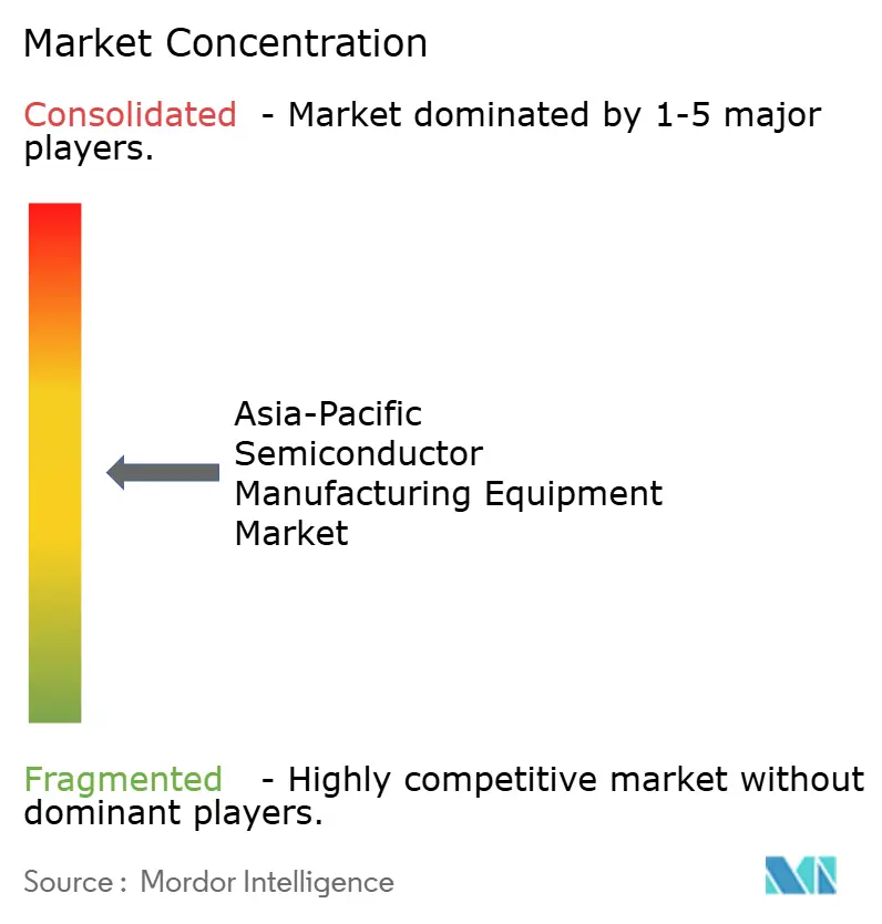
The Asia-Pacific semiconductor manufacturing equipment market is moderately concentrated, with higher concentration in advanced-process categories and greater diversity across mature-node, packaging, test, and specialty tools. Applied Materials, ASML, Lam Research, Tokyo Electron, and KLA have established positions in lithography, deposition, etch, and process control. Their systems are embedded in complex manufacturing flows and require extensive customer qualification. This gives established suppliers an advantage when tool uptime, process results, service support, and spare parts availability are essential. The broader supplier base is more diverse in mature-node and specialized equipment categories.
ASML reported in 2026 that High-NA EUV entered high-volume logic production with Intel Foundry's use of the TWINSCAN EXE:5200B system. This makes High-NA EUV a commercial manufacturing platform rather than only a qualification technology. Applied Materials partnered with TSMC at its EPIC Center in 2026 to work on materials engineering and process integration for AI-era scaling. Applied Materials also introduced new systems for DRAM and advanced packaging in 2026, including the SEMVision G7AP Defect Analysis system. These moves show suppliers seeking earlier involvement in customer process development and yield improvement.
Chinese equipment suppliers are focusing on mature-node and specialty categories where customer qualification can be more attainable than at the leading edge. Lam Research, ASML, and imec demonstrated High-NA EUV patterning work in 2026, showing the importance of cross-company process development for future nodes. Specialists such as SÜSS MicroTec, EV Group, Hanmi Semiconductor, DISCO, and ASMPT participate in packaging, bonding, dicing, and other specialized equipment areas. SEMI equipment reliability and environmental, health, and safety standards remain important in customer procurement and facility operations. The Asia-Pacific semiconductor manufacturing equipment market, therefore, remains competitive, with customers seeking new capabilities without compromising production stability.
Asia-Pacific Semiconductor Manufacturing Equipment Industry Leaders
-
Applied Materials, Inc.
-
ASML Holding N.V.
-
LAM RESEARCH CORPORATION
-
Tokyo Electron Limited
-
KLA Corporation
- *Disclaimer: Major Players sorted in no particular order
Recent Industry Developments
- July 2026: ASML announced that Intel Foundry became the first company to use High-NA EUV technology, TWINSCAN EXE:5200B, in high-volume logic chip production on the Intel 18A process node. This milestone marks the commercial transition of High-NA EUV from qualification to volume production deployment. It sets a key adoption benchmark for other advanced fabs considering orders for High-NA tools.
- June 2026: Applied Materials launched a suite of new chipmaking systems for advanced DRAM and packaging, including the SEMVision G7AP Defect Analysis system and multiple deposition platforms targeting 3D chip architectures for AI. The SEMVision G7AP was announced as already in production at leading logic manufacturers, accelerating yield learning for high-bandwidth memory and advanced packaging designs.
- May 2026: Applied Materials and TSMC announced a new R&D innovation partnership at Applied's USD 5 billion EPIC Center in Silicon Valley, with TSMC joining as a founding partner to co-develop materials engineering, next-generation equipment, and process integration technologies for the AI scaling era.
Asia-Pacific Semiconductor Manufacturing Equipment Market Report Scope
The Asia-Pacific Semiconductor Manufacturing Equipment Market Report is Segmented by Equipment Type (Wafer Fab Equipment / Front-End Equipment, and More), by Device Type (Logic and Micro-Components, Memory, Analog, and More), by End-User (Integrated Device Manufacturers (IDMs), Foundries, and More), and by Geography (China, Taiwan, Japan, and More). The Report Offers Market Size and Value (USD) Forecasts for all the Above Segments.
| Wafer Fab Equipment / Front-End Equipment (lithography, deposition, etching, cleaning, CMP, thermal processing, front-end metrology & inspection equipment, etc.) |
| Assembly and Packaging Equipment (die attach, wire bonding, flip-chip bonding, wafer bumping, thinning, dicing, molding, etc.) |
| Semiconductor Test Equipment (automated test equipment, wafer probers, test handlers, burn-in equipment, and final test equipment) |
| Fab Facility, Automation and Support Equipment (automation systems, wafer handling systems, AMHS, chemical & gas delivery systems, chillers, cleanroom support equipment, etc.) |
| Logic and Microcomponents (logic ICs, etc.) |
| Memory (DRAM, NAND, HBM, NOR, etc.) |
| Microprocessors (MPUs) |
| Analog (Power management ICs, signal chain, interface Ics, etc.) |
| Discrete and Power Devices (Diodes, transistors, MOSFETs, etc.) |
| Sensors, MEMS and Optoelectronic Devices (Image sensors, MEMS sensors, etc.) |
| Integrated Device Manufacturers (IDMs) |
| Foundries |
| Outsourced Semiconductor Assembly and Test (OSAT) Companies |
| Others (Research & Development (R&D) and Pilot Lines) |
| China |
| Taiwan |
| South Korea |
| Japan |
| Singapore |
| India |
| Rest of Asia-Pacific |
| By Equipment Type | Wafer Fab Equipment / Front-End Equipment (lithography, deposition, etching, cleaning, CMP, thermal processing, front-end metrology & inspection equipment, etc.) |
| Assembly and Packaging Equipment (die attach, wire bonding, flip-chip bonding, wafer bumping, thinning, dicing, molding, etc.) | |
| Semiconductor Test Equipment (automated test equipment, wafer probers, test handlers, burn-in equipment, and final test equipment) | |
| Fab Facility, Automation and Support Equipment (automation systems, wafer handling systems, AMHS, chemical & gas delivery systems, chillers, cleanroom support equipment, etc.) | |
| By Device Type | Logic and Microcomponents (logic ICs, etc.) |
| Memory (DRAM, NAND, HBM, NOR, etc.) | |
| Microprocessors (MPUs) | |
| Analog (Power management ICs, signal chain, interface Ics, etc.) | |
| Discrete and Power Devices (Diodes, transistors, MOSFETs, etc.) | |
| Sensors, MEMS and Optoelectronic Devices (Image sensors, MEMS sensors, etc.) | |
| By End User | Integrated Device Manufacturers (IDMs) |
| Foundries | |
| Outsourced Semiconductor Assembly and Test (OSAT) Companies | |
| Others (Research & Development (R&D) and Pilot Lines) | |
| By Geography | China |
| Taiwan | |
| South Korea | |
| Japan | |
| Singapore | |
| India | |
| Rest of Asia-Pacific |
Key Questions Answered in the Report
How large is the Asia-Pacific semiconductor manufacturing equipment market in 2026?
The Asia-Pacific semiconductor manufacturing equipment market is estimated at USD 101.4 billion in 2026 and is forecast to reach USD 181.0 billion by 2031. The forecast reflects continued investment in advanced logic, memory, packaging, and capacity localization.
What is driving equipment demand in Asia-Pacific semiconductor manufacturing?
AI computing, HBM capacity, advanced-node production, packaging investment, and government-backed fab programs are expanding equipment needs. These factors increase demand for lithography, deposition, etch, inspection, bonding, packaging, and test systems across regional manufacturing locations.
Why are AI chips increasing semiconductor equipment purchases?
AI chips need advanced logic, HBM, and complex packaging. These products require additional deposition, etch, bonding, inspection, and test tools, while larger HBM stacks also raise process complexity during memory manufacturing.
Which Asia-Pacific countries are important destinations for equipment investment?
China, Taiwan, South Korea, and Japan were the main equipment-spending locations in 2025. India, Singapore, and Malaysia also drive demand through manufacturing, packaging, specialty fabrication, research, and supply chain development programs.
How do export controls affect semiconductor equipment and suppliers?
Restrictions can change tool availability, product configurations, licensing needs, service plans, and customer sourcing decisions. They also encourage separate technology paths where access to advanced tools depends on policy conditions and supplier compliance.
Why is advanced packaging important for semiconductor manufacturing?
Advanced packaging combines multiple dies and memory components in dense systems. It creates demand for bonding, lithography, inspection, dicing, and test equipment, while manufacturers work to improve alignment, thermal performance, and production yield.