Asia-Pacific LED Epitaxial Wafer Market Size and Share
Market Overview
| Study Period | 2020 - 2031 |
|---|---|
| Forecast Data Period | 2026 - 2031 |
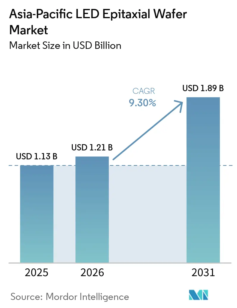
| Base Year Market Size (2025) | USD 1.13 Billion |
| Market Size (2026) | USD 1.21 Billion |
| Market Size (2031) | USD 1.89 Billion |
| Growth Rate (2026 - 2031) | 9.30% CAGR |
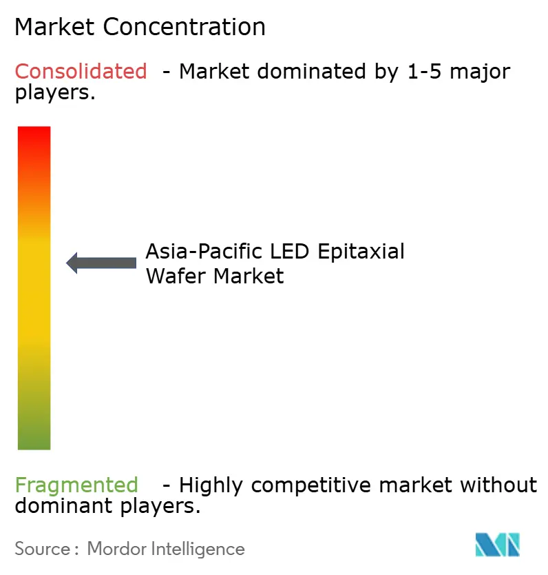
| Market Concentration | Medium |
Major Players *Disclaimer: Major Players sorted in no particular order Image © Mordor Intelligence. Reuse requires attribution under CC BY 4.0. | |
Asia-Pacific LED Epitaxial Wafer Market Analysis by Mordor Intelligence
The Asia-Pacific LED Epitaxial Wafer market size is expected to grow from USD 1.13 billion in 2025 to USD 1.21 billion in 2026 and is forecast to reach USD 1.89 billion by 2031 at 9.3% CAGR over 2026-2031. Strong policy incentives, surging Mini-LED and Micro-LED demand, and widening automotive qualification pipelines are collectively steering value away from commodity lighting toward premium, performance-dense applications. Vertically integrated suppliers continue to leverage captive sapphire-substrate capacity to moderate input-cost volatility, yet silicon-substrate penetration is climbing as 200 mm reactors mature. Order visibility remains tethered to display and automotive attachment rates, so manufacturers are balancing risk through diversified material recipes and longer-term substrate contracts. Capital-equipment lead times of 12-18 months are still a bottleneck, which heightens the strategic importance of early reactor reservations and joint-procurement frameworks.
Key Report Takeaways
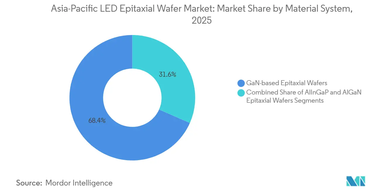
- By material system, GaN wafers led with a 68.4% share in 2025, while AlGaN is projected to expand at a 12.87% CAGR through 2031.
- By substrate type, sapphire accounted for 55.67% of the Asia-Pacific LED Epitaxial Wafer market share in 2025; silicon substrates recorded the fastest growth, with a 13.58% CAGR to 2031.
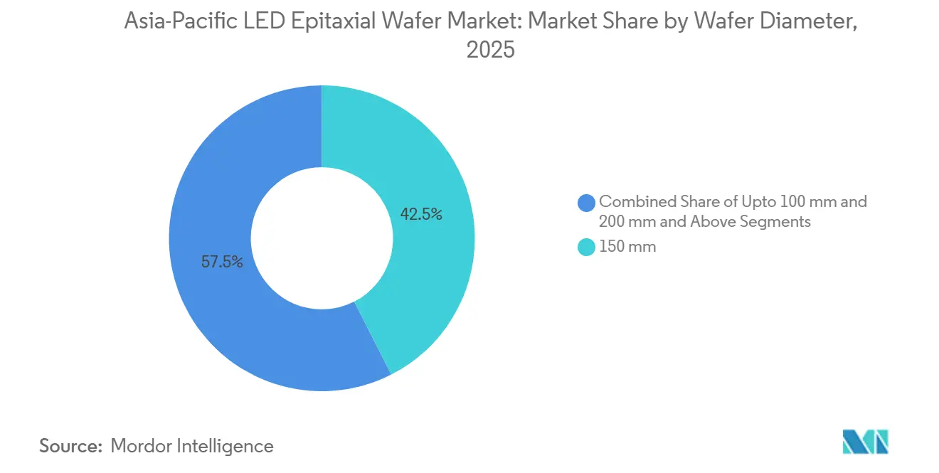
- By wafer diameter, the 150 mm segment accounted for 42.5% of the Asia-Pacific LED Epitaxial Wafer market in 2025, whereas the 200 mm-and-above category is advancing at a 13.16% CAGR.
- By application, general lighting accounted for 42.34% of revenue in 2025, yet displays and backlighting are forecast to post a 15.62% CAGR through 2031.
- By country, China captured 52.54% market share in 2025; India is on track for the highest CAGR among major economies, approximately 12.89%.
Note: Market size and forecast figures in this report are generated using Mordor Intelligence’s proprietary estimation framework, updated with the latest available data and insights as of January 2026.
Asia-Pacific LED Epitaxial Wafer Market Trends and Insights
Drivers Impact Analysis*
| DRIVER | (~) % IMPACT ON CAGR FORECAST | GEOGRAPHIC RELEVANCE | IMPACT TIMELINE |
|---|---|---|---|
| Government Subsidies for Regional Semiconductor Manufacturing | +2.10% | China, India, Japan, South Korea | Medium term (2-4 years) |
| Expansion of Micro-LED and Mini-LED Applications | +2.40% | China, South Korea, Japan, India | Medium term (2-4 years) |
| Rising Demand for High-Brightness Automotive Headlamps | +1.80% | China, Japan, South Korea, Rest of Asia-Pacific | Long term (≥ 4 years) |
| Rapid Urban Smart-Lighting Initiatives | +1.50% | India, China | Short term (≤ 2 years) |
| Advancements in GaN-on-SiC Wafer Yields | +1.20% | Japan, South Korea, China | Long term (≥ 4 years) |
| Growing Investments in UV-C LED Sterilization Systems | +0.90% | Japan, China, India | Medium term (2-4 years) |
| Source: Mordor Intelligence | |||
Expansion of Micro-LED and Mini-LED Applications
Active-matrix Mini-LED televisions reached 10% penetration in global shipments in 2026, compelling wafer makers to achieve wavelength binning tighter than ±2 nm across 6-inch substrates to avoid color-shift artifacts under HDR conditions. Tier-1 automakers have begun equipping high-end instrument clusters with Mini-LED backlights, reinforcing demand for low-defect GaN epitaxy. Samsung Display and LG Display are funding Micro-LED pilot lines for wearables, where each square meter of panel uses up to ten-times more wafer area than conventional LEDs, multiplying volume requirements.[5]Nichia Corporation, “280 nm Deep-UV LED Production,” nichia.co.jp Xiaomi’s 163-inch prototype validated scalability, contingent on mass-transfer yields below one-ppm defect rates. These projects elevate average selling prices because every performance drift incurs rework in downstream transfer processes.
Rising Demand for High-Brightness Automotive Headlamps
UNECE and updated Chinese GB regulations now allow adaptive-driving-beam modules that exceed 3 000 lumens while controlling glare. Nichia’s DominoPLS devices integrate 16 addressable segments per module, meeting both UNECE and GB photometric test requirements. India’s draft AIS-199 standard aligns with global norms, opening a new regional route for matrix headlamps. Automotive OEMs stipulate peak wavelengths at 450 nm ±5 nm and dislocation densities below 1 × 10^8 cm-2, pushing epitaxial houses toward larger sapphire or SiC substrates with advanced buffer stacks.
Rapid Urban Smart-Lighting Initiatives
Delhi, Hyderabad, and other municipalities are replacing legacy sodium fixtures with networked LED poles embedding traffic and air-quality sensors. Delhi’s 312 000-unit retrofit cuts power use by 55%, creating a predictable wafer pull-through for domestic fabs once local MOCVD tools are commissioned. Shanghai’s Pudong pilot added 5G small cells to 50 000 poles in 2025, showcasing blended telecom-lighting investment models. Such projects favor epitaxial wafers delivering efficacy above 180 lm/W at 85 °C junction temperatures.
Government Subsidies for Regional Semiconductor Manufacturing
National incentive programs are slashing payback periods for new epitaxial reactors from roughly 8 years to less than 5, prompting aggressive capacity additions even when end-market demand is cyclical.[1]Invest India, “India Semiconductor Mission,” investindia.gov.inIndia’s Semicon India Program covers up to half of fab outlays and requires local sourcing targets that redirect supply-chain spend into domestic firms. Japan’s multi-billion-dollar subsidy pool favors gallium-nitride and ultraviolet devices to reduce reliance on imported sapphire substrates.[2]Ministry of Economy, Trade and Industry, “Semiconductor Infrastructure Funding,” meti.go.jpSouth Korea’s decade-long mega-cluster plan positions LED epitaxy as an upstream feeder for Micro-LED display lines.[3]Ministry of Trade, Industry and Energy, “K-Semiconductor Strategy,” motie.go.kr In China, “Made in China 2025” funds expansion at Sanan Optoelectronics and HC Semitek, accelerating the shift toward larger-diameter tools.[4]State Council of China, “Made in China 2025 Roadmap,” gov.cn
Restraints Impact Analysis*
| RESTRAINT | (~) % IMPACT ON CAGR FORECAST | GEOGRAPHIC RELEVANCE | IMPACT TIMELINE |
|---|---|---|---|
| High Capital Expenditure for MOCVD Tools | -1.40% | China, India, Rest of Asia-Pacific | Short term (≤ 2 years) |
| Supply Chain Volatility of Sapphire Substrates | -1.10% | Global, acute in India and Rest of Asia-Pacific | Medium term (2-4 years) |
| Thermal Mismatch Challenges in Large-Diameter Silicon Wafers | -0.80% | China, Japan, South Korea | Long term (≥ 4 years) |
| Intellectual-Property Licensing Barriers for Start-ups | -0.60% | India, Rest of Asia-Pacific | Medium term (2-4 years) |
| Source: Mordor Intelligence | |||
Supply Chain Volatility of Sapphire Substrates
China will supply more than 40% of global sapphire ingots by 2026, but any export controls or logistical disruptions will instantly reverberate across Asia-Pacific fabs. Lead times stretch when smartphone camera-cover demand overlaps display peaks, sending 4-inch wafer prices swinging between USD 15 and USD 25 apiece. India’s PLI rules require 25% local substrate value within three years, yet no domestic ingot producer exists, forcing fabs to lock multi-year import contracts that dilute subsidy benefits.
High Capital Expenditure for MOCVD Tools
Batch reactors account for nearly half of a greenfield fab's budget, with single-tool prices ranging from USD 3 to 8 million. Veeco’s Lumina+ platform promises 15% higher throughput on 200 mm GaN-on-silicon but remains affordable only to vertically integrated firms or government-backed consortia. AIXTRON’s 2025 order book revealed delays as customers waited for clearer Mini-LED demand. India faces 20% import duties on equipment and lengthy paperwork under sovereign guarantees, slowing project approvals.
*Our forecasts treat driver/restraint impacts as directional, not additive. The impact forecasts reflect baseline growth, mix effects, and variable interactions.
Segment Analysis
By Material System: AlGaN Wafers Capture UV Premium
GaN wafers dominated 68.40% of shipments in 2025 on the back of general lighting, automotive, and display backlighting. The Asia-Pacific LED Epitaxial Wafer market size for AlGaN is projected to expand at 12.87% CAGR through 2031 as municipalities adopt mercury-free UV-C disinfection. Nichia’s 280 nm devices, delivering 7.4% wall-plug efficiency, validated commercial viability and sparked procurement from water-utility operators.
Pricing now bifurcates between commoditized GaN for bulbs and premium GaN or AlGaN wafers meeting ±2 nm wavelength uniformity and sub-1 cm-2 defect specs. Elevated aluminum fractions in AlGaN raise cracking risks, so producers are experimenting with aluminum-nitride buffer layers and pulsed lateral overgrowth. Material selection thus hinges on balancing throughput, epitaxial stress, and emerging UV demand, especially for healthcare sterilization.


By Substrate Type: Silicon Scaling Gains Momentum
Sapphire held 55.67% share in 2025 because of favorable lattice matching and mature reactor chemistries. Silicon substrates, growing at a 13.58% CAGR, leverage 200 mm wafer availability and semiconductor-grade metrology to reduce the cost per die. Innoscience demonstrated 97% yield on 8-inch GaN-on-silicon wafers after implementing graded AlGaN buffers and real-time stress monitoring.
Silicon carbide remains a niche due to a 3-5× cost premium, yet offers unmatched thermal conductivity for high-current LEDs. Gallium-arsenide serves red-amber AlInGaP but is diameter-limited. The Asia-Pacific LED Epitaxial Wafer market share balance, therefore, depends on whether display and automotive clients prioritize cost or thermal headroom.
By Wafer Diameter: 200 mm Segment Leads Efficiency Race
The legacy 150 mm format retained 42.5% volume in 2025 thanks to installed-base inertia, but 200 mm-plus wafers are on a 13.16% CAGR trajectory as reactor suppliers standardize chamber designs. Veeco’s TurboDisc architecture spreads precursor flow uniformly across 8-inch silicon, supporting lower defect densities that downstream transfer processes demand.
Diameter scaling, however, introduces wafer bow challenges exceeding 50 µm unless buffer gradients are tuned; closed-loop curvature control is fast becoming a qualification gate. Because each 200 mm wafer carries roughly 1.8× the die count of a 150 mm wafer, yield improvements rather than material savings drive adoption.
By Application: Displays Redefine Performance Benchmarks
General lighting retained a 42.34% share in 2025, buoyed by public-sector retrofits, yet displays and backlighting are set for a 15.62% CAGR as smartphone and television brands roll out Mini-LED local dimming above 10 000 zones. Automotive clusters now specify Mini-LED backlights rated for 1 000 000:1 contrast, which elevates epitaxial wavelength-uniformity requirements.
UV sterilization, though smaller, is accelerating with hospital and water-treatment mandates under the Minamata Convention. Industrial and specialty lighting, such as horticulture, provides a steady base load. Across these use cases, the Asia-Pacific LED Epitaxial Wafer market continues to segment into cost-per-lumen versus performance-per-square-millimeter value propositions.
Geography Analysis
China’s vertical integration from sapphire ingots to packaged chips underpins its 52.54% share, allowing aggressive pricing yet exposing overseas buyers to single-country risk. Sanan’s USD 239 million acquisition of Lumileds extended its Chinese reach into automotive qualifications and improved procurement leverage. Tight MOCVD utilization pushed wafer prices up to 15% between December 2025 and January 2026, underscoring supply elasticity challenges.
India’s growth story hinges on the INR 40 000 crore subsidy framework that de-risks capex and ties incentives to local content. Early municipal wins, such as Delhi’s 312 000 smart poles, demonstrate latent wafer demand that domestic fabs aim to capture once reactors arrive. Yet the absence of local sapphire capacity and 20% equipment duties may delay cost competitiveness until late-decade ramps.
Japan’s strategy is premium specialization. Nichia’s 7.4%-efficient 280 nm UV-C LEDs and adaptive-driving-beam modules showcase R&D depth. Cross-licensing with ams Osram in October 2025 reduced litigation exposure and solidified technology moats, but high labor costs keep mass-market volumes modest. South Korea leverages display majors, with Seoul Semiconductor’s package-free Mini-LEDs feeding both automotive and television pipelines. Smaller ASEAN nations are deploying tax credits, yet have not matched India’s scale or China’s vertical depth.
Competitive Landscape
Five vendors, Nichia, Epistar, Sanan Optoelectronics, Seoul Semiconductor, and Osram Opto, command roughly 55-65% of installed reactors, indicating a moderate concentration in the Asia-Pacific LED Epitaxial Wafer market. Vertical integration is the favored hedge: Sanan pairs in-house sapphire growth with downstream packaging to buffer volatility in precursor prices. Nichia’s deep-UV breakthrough opened sterilization revenue streams where few rivals can match 7%+ efficiency.
Patent portfolios serve as both a shield and a currency. The Nichia-Osram cross-license elevated entry barriers, forcing start-ups to negotiate costly access or confine themselves to uncrowded wavelength niches. Seoul Semiconductor’s WICOP architecture halves the number of assembly steps, lowering total cost while increasing epitaxial wafer demand per unit.
India’s forthcoming fabs could disrupt low-cost tiers if local reactors achieve yield parity. Meanwhile, Wolfspeed’s transition to 300 mm SiC may introduce a new substrate class for ultra-high-current LEDs, although price remains a hurdle. Competitive intensity will likely sharpen as automotive and display clients raise qualification thresholds for defect density and wavelength consistency.
Asia-Pacific LED Epitaxial Wafer Industry Leaders
Sanan Optoelectronics Co., Ltd.
HC Semitek Corporation
Nichia Corporation
Seoul Semiconductor Co., Ltd.
Ennostar Corporation
- *Disclaimer: Major Players sorted in no particular order

Recent Industry Developments
- March 2026: Wolfspeed secured USD 475.9 million in financing to accelerate the ramp of 300 mm SiC wafers, broadening substrate options for high-power LEDs.
- Jan 2026: Wolfspeed began 300 mm SiC wafer production at its Mohawk Valley site.
- January 2026: Nichia launched a mercury-free initiative anchored by its deep-UV LED portfolio.
- December 2025: Regional wafer prices climbed 3-15% amid tight MOCVD utilization and higher metal-organic precursor costs.


Asia-Pacific LED Epitaxial Wafer Market Report Scope
The Asia-Pacific LED Epitaxial Wafer Market Report is segmented by Material System (GaN-based Epitaxial Wafers, AlInGaP Epitaxial Wafers, and AlGaN Epitaxial Wafers), Substrate Type (Sapphire, Silicon, Silicon Carbide (SiC), and Gallium Arsenide (GaAs)), Wafer Diameter (Up to 100 mm, 150 mm, and 200 mm and Above), Application (General Lighting, Automotive Lighting, Displays and Backlighting, UV Sterilization, and Industrial and Specialty Lighting), and Country (China, India, Japan, South Korea, and Rest of the Asia-Pacific). The Market Forecasts are Provided in Terms of Value (USD).
| GaN-based Epitaxial Wafers |
| AlInGaP Epitaxial Wafers |
| AlGaN Epitaxial Wafers |
| Sapphire |
| Silicon |
| Silicon Carbide (SiC) |
| Gallium Arsenide (GaAs) |
| Upto 100 mm |
| 150 mm |
| 200 mm and Above |
| General Lighting |
| Automotive Lighting |
| Displays and Backlighting |
| UV Sterilization |
| Industrial and Specialty Lighting |
| China |
| India |
| Japan |
| South Korea |
| Rest of the Asia-Pacific |
| By Material System | GaN-based Epitaxial Wafers |
| AlInGaP Epitaxial Wafers | |
| AlGaN Epitaxial Wafers | |
| By Substrate Type | Sapphire |
| Silicon | |
| Silicon Carbide (SiC) | |
| Gallium Arsenide (GaAs) | |
| By Wafer Diameter | Upto 100 mm |
| 150 mm | |
| 200 mm and Above | |
| By Application | General Lighting |
| Automotive Lighting | |
| Displays and Backlighting | |
| UV Sterilization | |
| Industrial and Specialty Lighting | |
| By Country | China |
| India | |
| Japan | |
| South Korea | |
| Rest of the Asia-Pacific |


Key Questions Answered in the Report
What is the current and forecast value of the Asia-Pacific LED Epitaxial Wafer market?
The market is valued at USD 1.13 billion in 2025, rises to USD 1.21 billion in 2026, and is projected to reach USD 1.89 billion by 2031.
How quickly are silicon substrates gaining share?
Silicon wafers are expanding at roughly 13.58% CAGR as 200 mm reactor platforms mature and yield improve.
Why are 200 mm wafers favored over 150 mm in new automotive programs?
Larger diameters cut cost per known-good die and achieve tighter wavelength binning, both critical for adaptive-beam headlamps.
Which country is likely to challenge China’s dominance by 2031?
India, supported by large fiscal incentives and smart-lighting demand, aims to reach notable regional market share within the forecast period.
Page last updated on:


