AlGaN Deep-UV LED Epitaxial Wafer Market Size and Share
Market Overview
| Study Period | 2020 - 2031 |
|---|---|
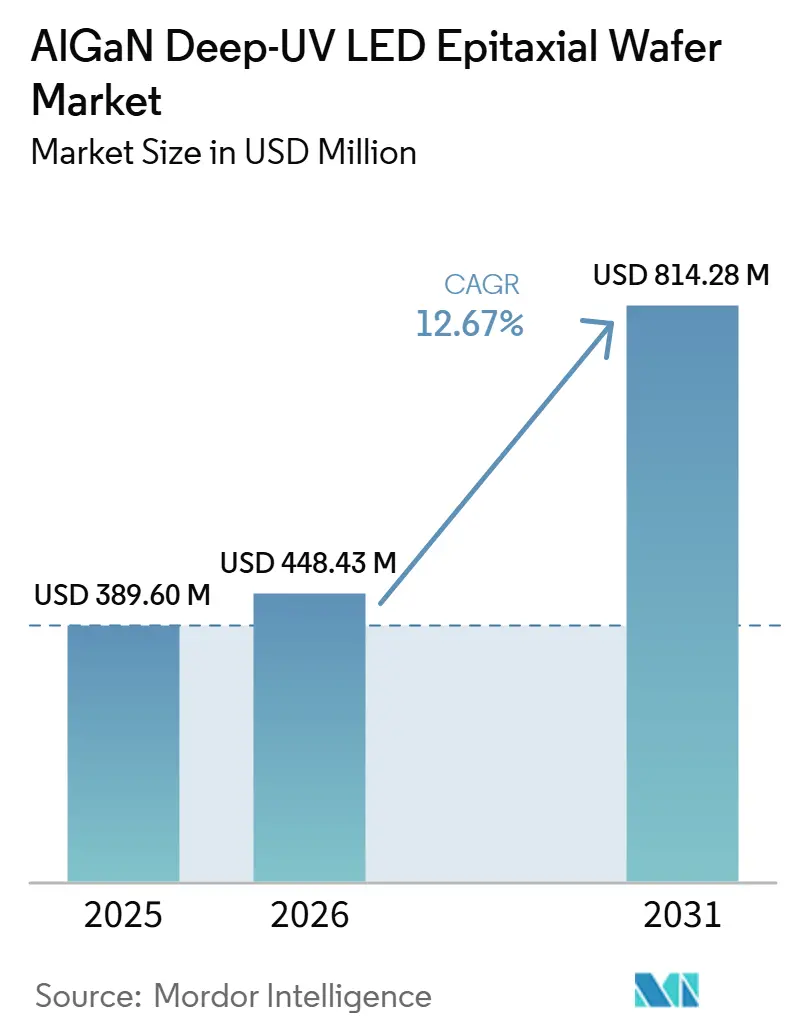
| Market Size (2026) | USD 448.43 Million |
| Market Size (2031) | USD 814.28 Million |
| Growth Rate (2026 - 2031) | 12.67% CAGR |
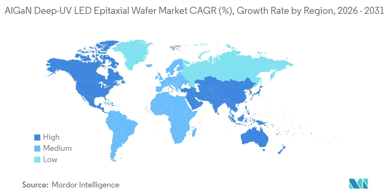
| Fastest Growing Market | North America |
| Largest Market | Asia Pacific |
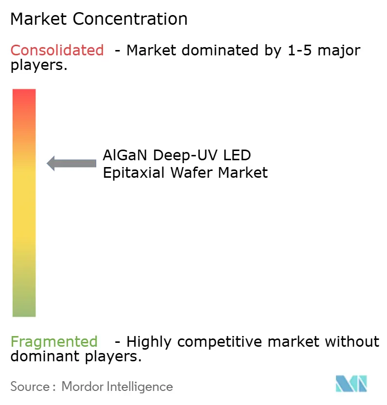
| Market Concentration | Medium |
Major Players *Disclaimer: Major Players sorted in no particular order Image © Mordor Intelligence. Reuse requires attribution under CC BY 4.0. | |
AlGaN Deep-UV LED Epitaxial Wafer Market Analysis by Mordor Intelligence
The AlGaN Deep-UV LED Epitaxial Wafer Market size is projected to expand from USD 389.60 million in 2025 and USD 448.43 million in 2026 to USD 814.28 million by 2031, registering a CAGR of 12.67% between 2026 to 2031. Heightened enforcement of mercury-lamp bans, sustained breakthroughs in tunnel-junction architectures, and the shift to 200 mm AlN-template substrates are catalyzing investment across Asia-Pacific and North America. Water utilities, consumer-electronics brands, and medical-device OEMs are simultaneously redesigning products around solid-state germicidal sources, reshaping long-standing mercury supply chains. Cost-per-watt parity remains elusive in large municipal plants, yet point-of-use and portable systems have crossed the inflection where lifetime economics favor LEDs. Competition pivots on external quantum efficiency gains below 270 nm, integration of patterned sapphire or AlN templates to cut dislocation density, and vertical integration that controls substrate, epitaxy, and packaging. As sovereign funding stimulates domestic fabs, the AlGaN deep-UV LED epitaxial wafer market is entering a phase where scale economics, not just laboratory efficiency records, will determine leadership.
Key Report Takeaways
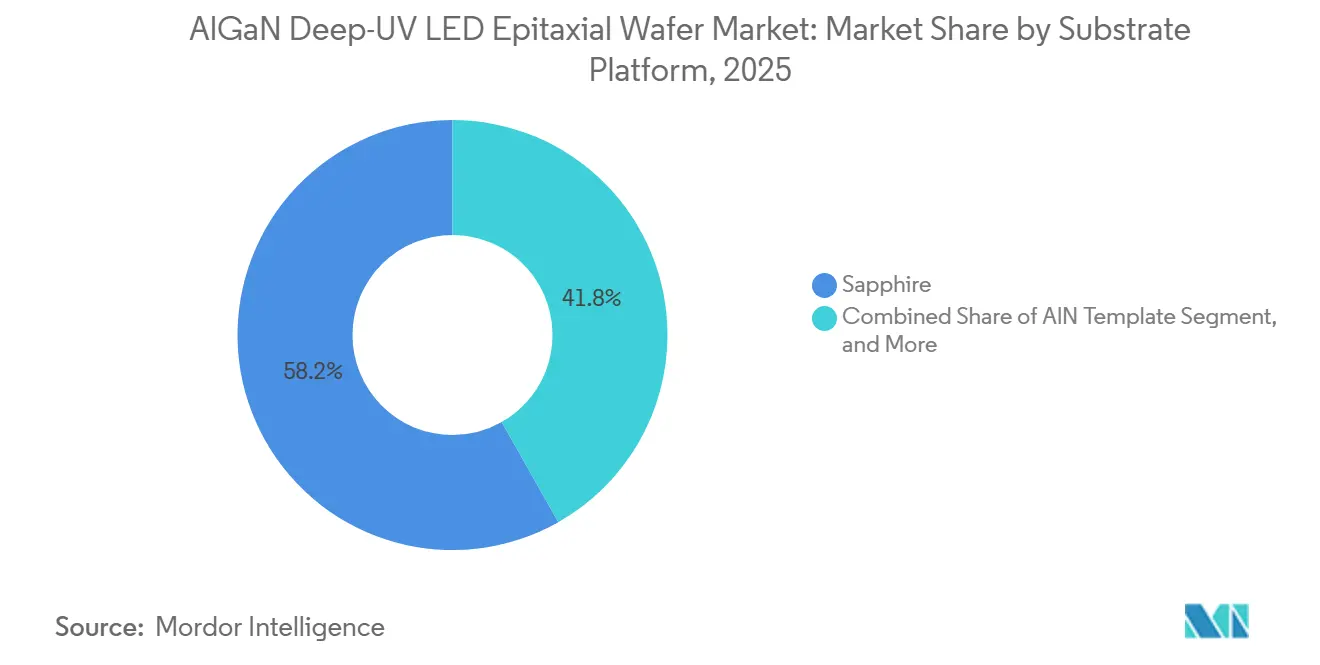
- By substrate platform, sapphire led with 58.19% revenue share in 2025, while AlN templates are projected to expand at a 13.28% CAGR to 2031.
- By wavelength band, UV-C held 46.14% of the AlGaN deep-UV LED epitaxial wafer market share in 2025 and is forecast to grow at a 13.86% CAGR through 2031.
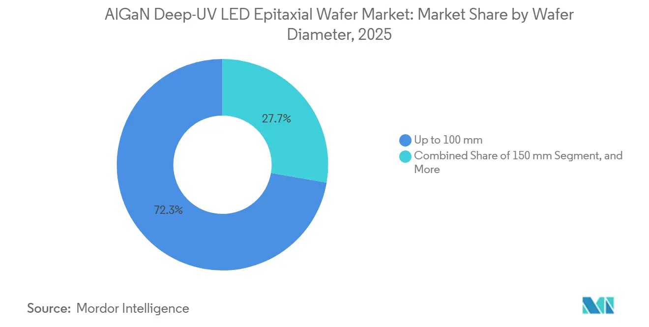
- By wafer diameter, up-to-100 mm wafers commanded 72.31% of the AlGaN deep-UV LED epitaxial wafer market size in 2025, whereas 200 mm and above is the fastest segment at a 13.91% CAGR through 2031.
- By application, water and air disinfection accounted for 41.29% of the AlGaN deep-UV LED epitaxial wafer market in 2025; medical and healthcare devices are advancing at a 13.98% CAGR through 2031.
- By geography, Asia-Pacific captured 55.83% of demand in 2025, but North America records the highest projected CAGR at 12.93% to 2031.
Note: Market size and forecast figures in this report are generated using Mordor Intelligence’s proprietary estimation framework, updated with the latest available data and insights as of January 2026.
Global AlGaN Deep-UV LED Epitaxial Wafer Market Trends and Insights
Drivers Impact Analysis*
| Driver | (~) % Impact on CAGR Forecast | Geographic Relevance | Impact Timeline |
|---|---|---|---|
| Regulatory bans on mercury UV lamps | +3.2% | Global, early in EU and North America | Short term (≤ 2 years) |
| Growing demand for point-of-use water disinfection | +2.8% | Global, focused in North America and Asia-Pacific homes | Medium term (2-4 years) |
| Tunnel-junction designs lowering forward voltage | +2.1% | Global, led by Japan and United States R and D centers | Medium term (2-4 years) |
| Patterned sapphire substrates optimized for UVC | +1.9% | Asia-Pacific core, adoption in North America and Europe | Long term (≥ 4 years) |
| Integration into semiconductor lithography tools | +1.5% | Asia-Pacific and North America advanced-node fabs | Long term (≥ 4 years) |
| Sovereignty programs funding domestic DUV fabs | +1.2% | China, Japan, United States | Long term (≥ 4 years) |
| Source: Mordor Intelligence | |||
Regulatory Bans on Mercury UV Lamps
Mandatory phase-outs of mercury-containing lamps in the European Union by December 2025 and the final RoHS exemption ending in February 2027 compel utilities and OEMs to adopt solid-state modules.[1]European Commission, “Mercury Regulation and RoHS Exemptions,” EUROPA.EU The Minamata Convention reinforces the global baseline, ensuring adoption pressure even in export-driven Asian manufacturing hubs. Nichia’s mercury-free disinfection initiative, launched in November 2025, demonstrates how vertically integrated suppliers are realigning internal operations to comply with the initiative. Near-term deployments concentrate on point-of-use systems below 100 W where retrofit costs are limited, while megawatt-scale municipal upgrades remain capital-intensive. Consequently, procurement cycles for the AlGaN deep-UV LED epitaxial wafer market are front-loaded into residential and portable devices before cascading into industrial retrofits.
Growing Demand for Point-of-Use Water Disinfection
Rising concerns about pathogens in tap water and in off-grid settings are fueling demand for compact UV-C purifiers powered by 265-280 nm LEDs. Chip-on-board modules based on AlGaN epitaxial wafers now deliver 145 mW at 275 nm in packages under 5.2 mm², enabling battery-powered designs. Asia-Pacific households facing boil-water advisories are early adopters, and disaster-relief agencies specify lightweight LED units for field deployment. Each purifier integrates multiple chips to deliver 40 mJ/cm² doses, thereby reducing wafer consumption despite smaller die sizes. As volumes rise, wafer producers optimize reactor throughput for 100 mm sapphire runs, creating a cost floor that challenges AlN templates in mid-power segments.
Tunnel-Junction Designs Lowering Forward Voltage
Transparent tunnel junctions demonstrated a 3.5 V reduction at 400 A/cm² compared with p-GaN contacts, reducing resistive losses and junction temperature.[2]Applied Physics Letters, “Multi-Active-Region AlGaN UV LEDs with Transparent Tunnel Junctions,” AIP.ORG Current spreading improves because the absorbing p-GaN layer is replaced by a doped n-type stack that transmits deep-UV photons. Flip-chip packages benefit most, as lower forward voltages translate directly to cooler operation and longer lifetime. Violumas’ March 2025 devices leveraged similar contacts for a 35-50% radiant-flux boost at 275 nm and 265 nm. Commercial roll-out hinges on precise Mg and Si doping controls inside MOCVD chambers, a hurdle that reactor vendors aim to solve before 2028.
Patterned Sapphire Substrates Optimized for UVC
Nanoscale patterns etched into sapphire mitigate total internal reflection and reduce dislocation density to 1.8 × 10⁶ cm⁻², raising the external quantum efficiency by up to 57.3%. Hybrid conical-hemispherical motifs relax lattice strain during AlGaN growth, enhancing deep-UV photon extraction. Although patterning inflates substrate costs by 20-30%, LED makers accept the premium because optical power directly drives the bill of materials in compact modules. Stanley Electric’s vertically integrated 265 nm line exemplifies the move to in-house patterned substrates to differentiate on performance. The trend is lifting long-term demand for high-grade patterned wafers in the AlGaN deep-UV LED epitaxial wafer market.
Restraints Impact Analysis*
| Restraint | (~) % Impact on CAGR Forecast | Geographic Relevance | Impact Timeline |
|---|---|---|---|
| High USD/W output cost versus mercury lamps | -2.5% | Global, acute in municipal and industrial retrofits | Short term (≤ 2 years) |
| Low EQE at 250-270 nm | -1.8% | Global, influences all deep-UV segments | Medium term (2-4 years) |
| Thermal management limits of flip-chip layouts | -1.1% | Global, focused on high-power arrays | Medium term (2-4 years) |
| Limited availability of bulk AlN substrates | -0.9% | Supply centered in United States and Japan | Long term (≥ 4 years) |
| Source: Mordor Intelligence | |||
High USD/W Output Cost Versus Mercury Lamps
At multimegawatt scales, UV-C LED systems still cost two-to-four times more per watt than legacy mercury lamps, lengthening payback to over seven years in budget-constrained utilities. Epitaxial wafer costs account for nearly half of device costs, so every incremental gain in EQE directly lowers module pricing. Nichia’s December 2024 280 nm device hit 7.4% wall-plug efficiency yet remains targeted at premium disinfection niches, highlighting the gap to mass municipal adoption.[3]Nichia Corporation, “Mercury-Free UV Disinfection Project,” NICHIA.CO.JP Asia-Pacific utilities, operating on tight margins, postpone large-scale conversions until wafer prices fall or subsidies become available. The constraint is therefore most severe in the near term for the AlGaN deep-UV LED epitaxial wafer market.
Low EQE at 250-270 nm
Production LEDs below 270 nm often have external quantum efficiencies below 4%, a ceiling imposed by high Mg activation energies, threading dislocations, and optical-mode polarization. While laboratories reported 10% at 275 nm on optimized AlN templates, reproducibility on high-throughput reactors remains elusive. Degradation compounds the hurdle, with hydrogen migration and point defects driving 30% lumen depreciation after 10 000 hours. Violumas’ 3-PAD thermal design slows decay but cannot offset fundamental EQE limits. Until volume lines cross the 8-10% threshold, LED modules will remain confined to use cases where mercury restrictions or form-factor constraints override cost.
*Our forecasts treat driver/restraint impacts as directional, not additive. The impact forecasts reflect baseline growth, mix effects, and variable interactions.
Segment Analysis
By Substrate Platform: Efficiency Gains Push AlN Adoption
The AlGaN deep-UV LED epitaxial wafer market, attributed to sapphire, reached USD 0.23 billion in 2025, accounting for 58.19% share, while AlN templates are projected to expand at a 13.28% CAGR, lifting their revenue contribution to more than USD 0.26 billion by 2031. Sapphire’s dominance stems from mature supply, reactor recipes, and favorable pricing, yet its high threading-dislocation density suppresses deep-UV efficiency. AlN’s lattice-matched growth slashes defect density below 10⁶ cm⁻², yielding consistent EQE improvements of 20-30%. HexaTech’s launch of 3-inch AlN in February 2026 and Crystal IS achieving 99% usable area on 100 mm wafers in June 2024 signpost scale-up momentum.
Migration is uneven across wavelengths. UV-A and UV-B devices retain sapphire because their lower aluminum content tolerates defects, whereas UV-C below 270 nm increasingly mandates AlN templates to attain usable power levels. Cost differentials are narrowing as wafer makers prepare 150 mm AlN lines that promise a 30% lower cost per die than today’s 100 mm blanks. Success will recalibrate sourcing strategies across the AlGaN deep-UV LED epitaxial wafer market, with vertically integrated players internalizing AlN growth to protect intellectual property and margins.


By Wavelength Band: UV-C Leads Growth Curve
UV-C wafers generated 46.14% revenue or USD 0.18 billion in 2025 and are accelerating at a 13.86% CAGR. Their germicidal peak at 265 nm aligns with water, air, and surface sterilization standards. Nichia’s mass-production ramp of 280 nm chips delivering 263 mW at 700 mA underscores commercial readiness. UV-A targets curing and counterfeit detection, enjoying higher EQE above 35% but slower volume growth due to mature lamp competition. UV-B supports dermatological therapy and horticulture; regulatory approvals constrain scaling, yet premium pricing offsets lower unit counts.
Far-UVC below 240 nm remains a frontier in R&D. Silanna UV advanced 233 nm devices that double radiant intensity to 2 mW/sr, hinting at future occupied-space disinfection. However, aluminum fractions above 60% elevate strain and defect sensitivity, hindering yields. Overall, wavelength segmentation reflects application pull: disinfection drives UV-C demand while industrial sensors push niche far-UVC volumes, collectively shaping design specs within the AlGaN deep-UV LED epitaxial wafer market.
By Wafer Diameter: 200 mm Transition Gains Pace
Up-to-100 mm wafers held 72.31% share equal to USD 0.28 billion in 2025, yet 200 mm blanks are tracking a 13.91% CAGR through 2031. Spreading epitaxial cost across 8-to-10× more dies lowers per-chip expense by up to 50% under yield-parity assumptions. Reactor vendors now ship multi-wafer tools capable of three 200 mm substrates per run, matching semiconductor fabs’ cleanroom flows. Early 200 mm sapphire lots report yields 10-15 percentage points below 100 mm, muting immediate savings, but process learning curves echo historic GaN-on-Si ramps and are expected to converge by 2028.
AlN remains limited to 100 mm, constraining UV-C makers that require dislocation suppression. Consequently, the first 200 mm adopters reside in UV-A and UV-B portfolios or mixed-material stacks that tolerate defect levels. As AlN suppliers scale to 150 mm, a hybrid migration path emerges. OEMs hedge risk by qualifying both 150 mm AlN and 200 mm sapphire, keeping supply flexible while chasing cost benchmarks central to the AlGaN deep-UV LED epitaxial wafer industry.
By Application: Medical Devices Accelerate
Water and air disinfection modules generated 41.29% of 2025 revenue, leveraging compact LED arrays in residential under-sink units and HVAC retrofits. Medical and healthcare devices, while smaller in base, will post the fastest 13.98% CAGR as surgical-instrument cabinets and in-room purifiers gain regulatory clearance. Published clinical trials documenting 99.9% pathogen reduction in operating theaters fuel procurement budgets, particularly in North America. Surface sterilization for food-processing conveyors follows, with LED instant-on replacing hot cathode lamps and eliminating the risk of mercury contamination.
Industrial and analytical instruments command high margins per wafer, demanding tight wavelength tolerances for spectroscopy. Violumas’ ultra-narrow 10-degree beam optics exemplify customization that justifies premium pricing. Although such equipment consumes fewer wafers, its rigorous specifications push material and epitaxial process control, advancing technology that later diffuses into mass-market segments, reinforcing innovation cycles across the AlGaN deep-UV LED epitaxial wafer market.
Geography Analysis
Asia-Pacific generated USD 0.22 billion in AlGaN deep-UV LED epitaxial wafer revenue in 2025, accounting for 55.83% of global demand, largely because vertically integrated Japanese and South Korean suppliers control substrate growth, epitaxy, and device packaging. Japanese producers such as Nichia and Nikkiso capitalize on decades of MOCVD know-how, while South Korean firms leverage expansive patent portfolios to secure long-term contracts with consumer-electronics and water-treatment OEMs. China’s domestic semiconductor strategy also injects capital into compound-semiconductor lines, yet export controls on MOCVD tools and precursor gases continue to delay volume ramps for high-performance UV-C wafers. The region further benefits from government incentives that subsidize patterned-sapphire and AlN substrates, giving fabs an immediate cost advantage over overseas rivals. As a result, Asia-Pacific remains the primary manufacturing hub for the AlGaN deep-UV LED epitaxial wafer market through at least 2028.
North America recorded USD 0.09 billion in 2025 sales and is poised for a 12.93% CAGR through 2031, as the CHIPS Act provides funding for new AlN-substrate plants, reactor installations, and backend packaging lines. Domestic buyers in the medical and aerospace industries demand high-reliability UV-C devices that meet FDA and IEC safety criteria, encouraging local sourcing to reduce supply-chain risk. Several U.S. fabs are retrofitting 200 mm MOCVD reactors borrowed from GaN power-device lines, accelerating qualification timelines and lowering per-die costs. Research universities and national labs provide metrology support for tunnel-junction and far-UVC development, feeding a pipeline of proprietary process recipes. This ecosystem alignment positions North America as the fastest-growing regional buyer of high-specification wafers during the forecast window.
Europe commands a smaller share yet benefits from stringent mercury-lamp bans that drive solid-state retrofits across municipal water facilities. Germany and France support compound-semiconductor pilot lines through national innovation funds, but fragmented value chains limit economies of scale. Rest-of-World demand spanning the Middle East, Africa, and Latin America remains nascent, constrained by limited local manufacturing and reliance on imported modules. However, desalination projects in the Gulf and portable disinfection devices in South America are emerging as early adopters once cost parity improves. As sovereign programs worldwide encourage domestic wafer output, regional specialization intensifies, reshaping trading patterns within the AlGaN deep-UV LED epitaxial wafer market.

Competitive Landscape
The AlGaN deep-UV LED epitaxial wafer market is moderately concentrated, with five Japanese and South Korean leaders accounting for roughly 70% of installed capacity and defending their positions through vertical integration and expansive patent portfolios. Nichia, Nikkiso, Seoul Viosys, Stanley Electric, and Nitride Semiconductors supply patterned substrates, MOCVD processes, and packaged LEDs from single campuses, enabling tight yield control and rapid iteration of tunnel-junction designs. Their scale secures favorable pricing on sapphire and high-purity ammonia, giving them a structural cost edge over smaller challengers.
Emerging players focus on white-space niches to sidestep incumbent strengths. Silanna UV targets far-UVC wavelengths below 240 nm with hermetic packages suitable for occupied-space air purification, while Violumas focuses on ultra-narrow-beam optics for spectroscopy and fiber-coupled instruments. Crystal IS and HexaTech vertically integrate AlN substrate production, capturing margin and mitigating supply shortages that hamper many fabless device companies. U.S. and European startups often partner with domestic universities to share pilot reactors and accelerate qualification without heavy capital outlay.
Patent barriers remain formidable, especially around Violed's surface treatments and transparent tunnel-junction contacts. New entrants, therefore, emphasize proprietary substrate engineering or specialized packaging rather than frontal assaults on core LED architectures. Government procurement preferences for locally made semiconductor components further fragment competition along geographic lines, elevating the importance of regional manufacturing footprints. Collectively, these dynamics sustain a market where leadership rests on both technological differentiation and strategic control of critical materials, ensuring that no single firm achieves overwhelming dominance in the AlGaN deep-UV LED epitaxial wafer market.
AlGaN Deep-UV LED Epitaxial Wafer Industry Leaders
Nitride Semiconductors Co., Ltd.
Seoul Viosys Co., Ltd.
Nichia Corporation
Crystal IS, Inc.
Sensor Electronic Technology, Inc.
- *Disclaimer: Major Players sorted in no particular order

Recent Industry Developments
- March 2026: HexaTech launched 3-inch AlN substrates and confirmed a fast-track to 100 mm production, citing defect densities below 1 × 10⁶ cm⁻².
- March 2026: Violumas released next-gen 255 nm, 265 nm, and 275 nm LEDs in SMD and COB formats, boosting radiant flux by up to 30% versus prior parts.
- January 2026: Violumas showcased a full UV LED lineup at Photonics West, previewing an upgraded 3535 series with 10-degree beam optics slated for Q2 2026.
- September 2025: Silanna UV unveiled the SF2 far-UVC LED at 233 nm, doubling radiant intensity and delivering hermetically sealed TO-39 packaging.


Global AlGaN Deep-UV LED Epitaxial Wafer Market Report Scope
The AlGaN Deep-UV LED Epitaxial Wafer Market Report is Segmented by Substrate Platform (Sapphire, AlN Template, Silicon Carbide (SiC), Other Substrate Platforms), Wavelength Band (UV-A (315-400 nm), UV-B (280-315 nm), UV-C (200-280 nm)), Wafer Diameter (Up to 100 mm, 150 mm, 200 mm and Above), Application (Water and Air Disinfection, Surface Sterilisation, Medical and Healthcare Devices, Industrial and Analytical Instruments), and Geography (North America, Europe, Asia-Pacific, Rest of the World). The Market Forecasts are Provided in Terms of Value (USD).
| Sapphire |
| AlN Template |
| Silicon Carbide (SiC) |
| Other Substrate Platforms |
| UV-A (315-400 nm) |
| UV-B (280-315 nm) |
| UV-C (200-280 nm) |
| Up to 100 mm |
| 150 mm |
| 200 mm and Above |
| Water and Air Disinfection |
| Surface Sterilisation |
| Medical and Healthcare Devices |
| Industrial and Analytical Instruments |
| North America |
| Europe |
| Asia-Pacific |
| Rest of the World |
| By Substrate Platform | Sapphire |
| AlN Template | |
| Silicon Carbide (SiC) | |
| Other Substrate Platforms | |
| By Wavelength Band | UV-A (315-400 nm) |
| UV-B (280-315 nm) | |
| UV-C (200-280 nm) | |
| By Wafer Diameter | Up to 100 mm |
| 150 mm | |
| 200 mm and Above | |
| By Application | Water and Air Disinfection |
| Surface Sterilisation | |
| Medical and Healthcare Devices | |
| Industrial and Analytical Instruments | |
| By Geography | North America |
| Europe | |
| Asia-Pacific | |
| Rest of the World |


Key Questions Answered in the Report
What is the projected value of the AlGaN deep-UV LED epitaxial wafer market by 2031?
The market is forecast to reach USD 0.81 billion by 2031, expanding at a 12.67% CAGR from 2026-2031.
Which substrate platform is growing the fastest?
AlN templates show the fastest growth, advancing at a 13.28% CAGR thanks to lower dislocation densities that lift efficiency.
Why are UV-C wafers outpacing UV-A and UV-B growth?
Mercury-lamp bans and rising demand for germicidal disinfection push UV-C wafers forward, leading to a 13.86% CAGR through 2031.
How does wafer diameter affect cost?
Moving from 100 mm to 200 mm spreads epitaxial costs over more die, potentially halving per-chip expense once yields converge.
Which region will be the fastest-growing buyer of deep-UV wafers?
North America leads in growth with a projected 12.93% CAGR as CHIPS Act incentives finance local substrate and epitaxy lines.
What is the main technical barrier to wider adoption?
Low external quantum efficiency below 270 nm keeps cost per watt high, limiting penetration in large industrial systems.
Page last updated on:


