
Advanced DRAM Packaging Market Size and Share
Market Overview
| Study Period | 2020 - 2031 |
|---|---|
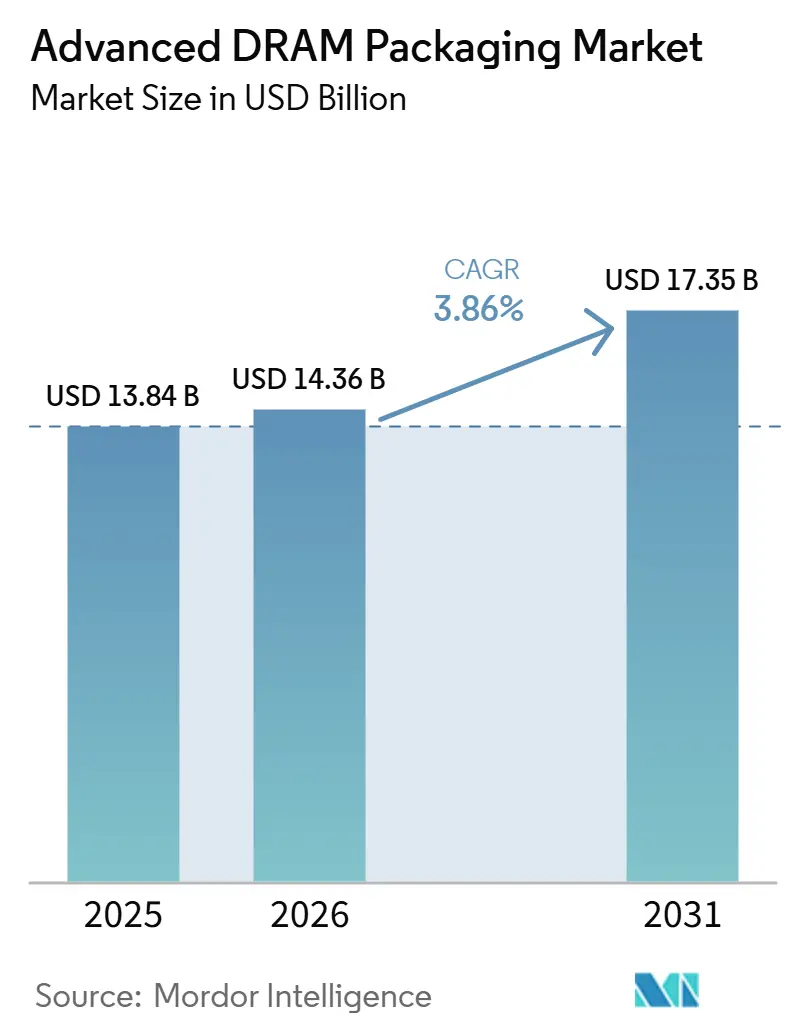
| Market Size (2026) | USD 14.36 Billion |
| Market Size (2031) | USD 17.35 Billion |
| Growth Rate (2026 - 2031) | 3.86 % |
| Fastest Growing Market | North America |
| Largest Market | Asia-Pacific |
| Market Concentration | Medium |
Major Players *Disclaimer: Major Players sorted in no particular order Image © Mordor Intelligence. Reuse requires attribution under CC BY 4.0. | |
Advanced DRAM Packaging Market Analysis by Mordor Intelligence
The advanced DRAM packaging market size was USD 13.84 billion in 2025, USD 14.36 billion and is forecast to reach USD 17.35 billion by 2031 at a CAGR of 3.86% over 2026-2031. Growth in the advanced DRAM packaging market reflects a clear shift in semiconductor value creation, where packaging has become the main performance lever for AI compute systems rather than smaller transistor geometry. The advanced DRAM packaging market is being shaped by co-designed memory, substrate, interposer, and stacking requirements that must deliver very high bandwidth inside tightly managed thermal envelopes. This change has moved advanced DRAM packaging from a back-end manufacturing step into a strategic control point across AI infrastructure build-outs and semiconductor supply chain realignment. Asia-Pacific remains central because DRAM fabrication, OSAT infrastructure, and substrate supply are concentrated there, while North America is gaining momentum through localization programs and new packaging investments. The market is still constrained by capital intensity, yield sensitivity, and substrate shortages, which means qualified suppliers in the advanced DRAM packaging market continue to hold stronger pricing power than would be expected in a purely demand-led cycle.
Key Report Takeaways
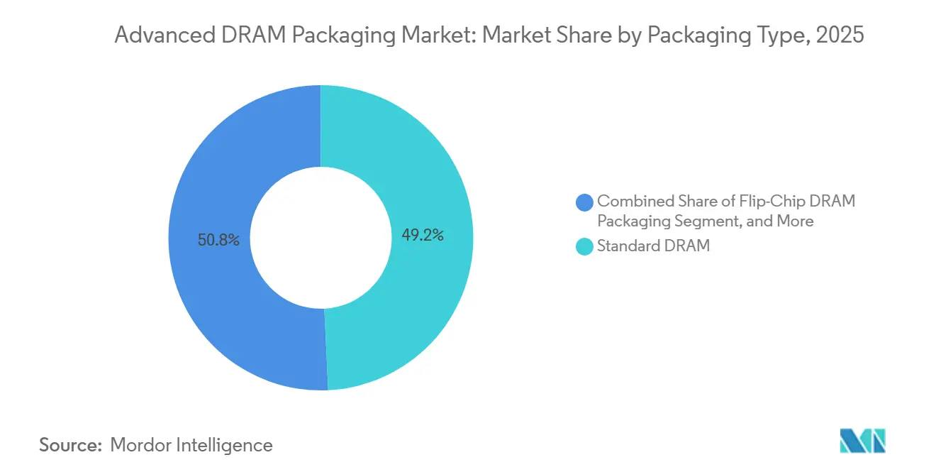
- By packaging type, standard DRAM packaging led with 49.67% revenue share in 2025, while HBM packaging within the Others category is projected to expand at a 4.48% CAGR through 2031.
- By integration technology, wire bonding held 47.45% share of the advanced DRAM packaging market in 2025, while TSV-based stacking is projected to record the highest CAGR at 4.52% through 2031.
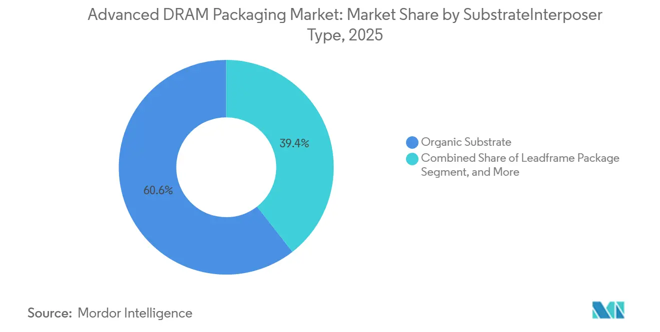
- By substrate and interposer type, organic substrates accounted for 60.56% of revenue in 2025, while silicon interposer and TSV-based interconnect is projected to grow at a 4.78% CAGR through 2031.
- By ecosystem channel, DRAM manufacturers controlled 41.45% of revenue in 2025, while advanced packaging foundries are projected to expand at a 4.67% CAGR through 2031.
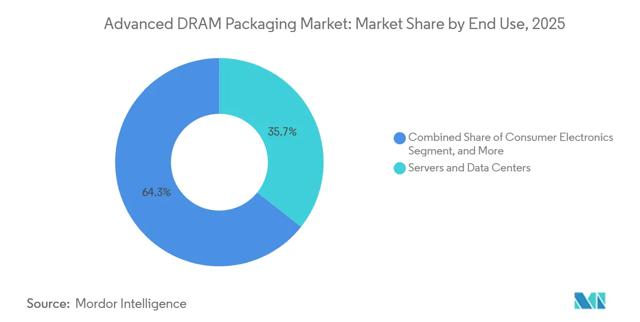
- By end use, servers and data centers accounted for 35.78% share of the advanced DRAM packaging market in 2025 and are projected to grow at a 4.52% CAGR through 2031.
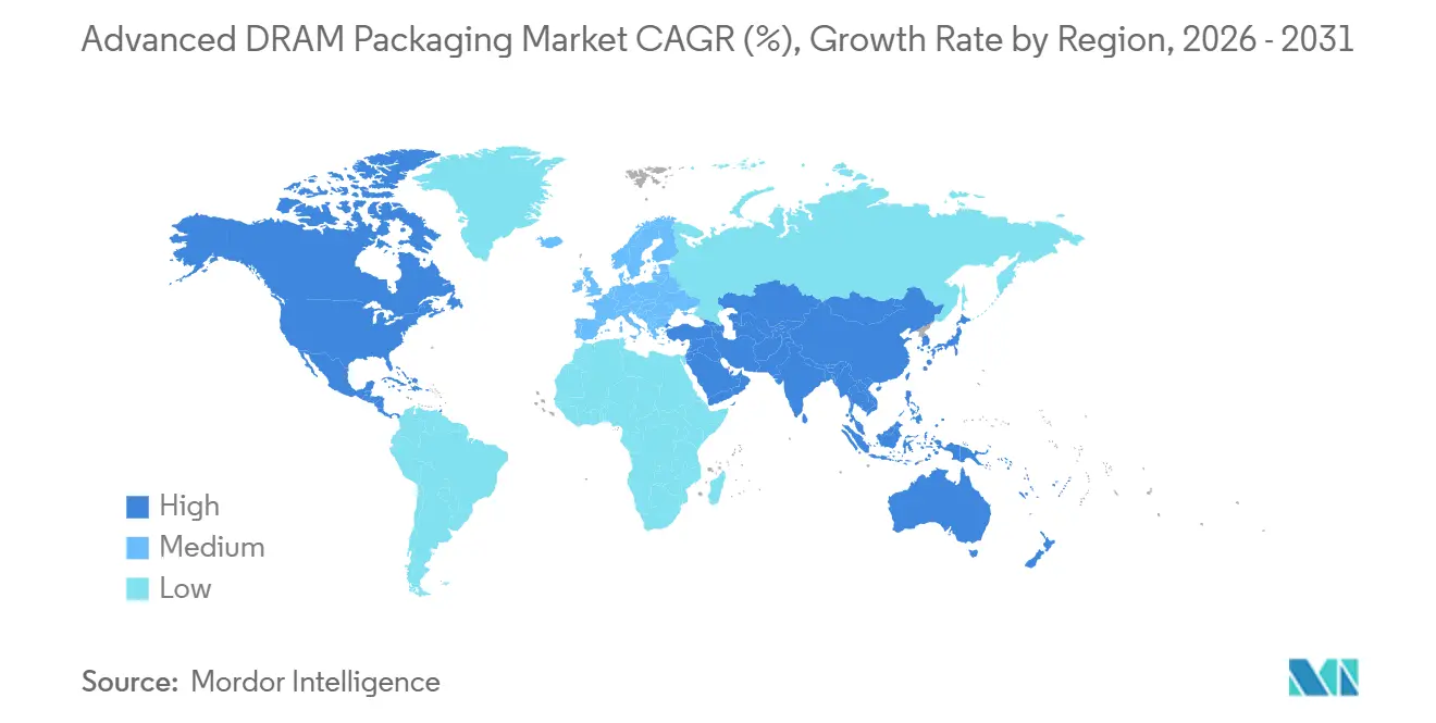
- By geography, Asia-Pacific held 85.43% of the advanced DRAM packaging market share in 2025, while North America is projected to record the fastest regional CAGR at 4.67% through 2031.
Note: Market size and forecast figures in this report are generated using Mordor Intelligence’s proprietary estimation framework, updated with the latest available data and insights as of January 2026.
Market Trends and Insights
Drivers Impact Analysis of Advanced DRAM Packaging Market*
| Driver | (~) % Impact on CAGR Forecast | Geographic Relevance | Impact Timeline |
|---|---|---|---|
| Rising AI Server Memory Density Requirements | +1.5% | Global, with intensity in Asia-Pacific and North America | Short term (≤ 2 years) |
| Transition to Higher Bandwidth Memory Architectures | +1.2% | South Korea, Taiwan, spill-over to North America | Medium term (2-4 years) |
| Heterogeneous Integration Demand in Advanced Nodes | +0.7% | Global, concentration in Taiwan and North America | Medium term (2-4 years) |
| Expanding Outsourced Advanced Packaging Capacity | +0.5% | Asia-Pacific core, spill-over to North America | Medium term (2-4 years) |
| Government Incentives for Semiconductor Supply Chain Localization | +0.4% | North America, Europe, Japan, South Korea | Long term (≥ 4 years) |
| Thermal and Signal Integrity Constraints in High-Performance DRAM | +0.3% | Global | Long term (≥ 4 years) |
| Source: Mordor Intelligence | |||
Rising AI Server Memory Density Requirements
AI server deployment is pushing each compute platform to carry much more packaged memory than earlier accelerator generations. That shift is making the advanced DRAM packaging market more dependent on higher stack heights, denser interconnects, and stricter thermal control inside each package. Samsung shipped 12-layer HBM4E samples with 48GB capacity and 3.6TB/s per-stack bandwidth in May 2026, which shows how memory density and bandwidth are moving higher at the same time.[1] As more hyperscalers build custom accelerators, the number of qualified customers for advanced bonding and stacking flows is also widening across the advanced DRAM packaging market. That broadens volume demand beyond a narrow GPU base and creates steadier pull for OSATs and vertically integrated memory suppliers that can support high-density packaging programs. The result is that the advanced DRAM packaging market is seeing demand growth not just from more servers, but from more memory content and more complex package structures inside each server platform.
Transition To Higher Bandwidth Memory Architectures
The move from HBM3E to HBM4 is raising the technical threshold for every qualified supplier in the advanced DRAM packaging market. JEDEC published the HBM4 standard in April 2025 with a 2,048-bit interface, which doubled the width from HBM3 and lifted packaging demands across routing, signal integrity, and controller design.[2]Those requirements are steering design wins toward silicon interposers and more advanced build-up substrates because conventional organic formats cannot manage the same routing burden at similar performance levels. HBM4 also requires a new controller approach, so packaging teams with established co-design relationships gain a meaningful lead in qualification cycles. SK hynix confirmed a KRW 19 trillion investment, equivalent to USD 12.85 billion, for its packaging facility in Cheongju in early 2026, which underlines how the advanced DRAM packaging market is absorbing capital to support this architecture shift. This migration is not a simple product refresh, because it changes the package, the substrate choice, the controller, and the supplier qualification path at the same time.
Heterogeneous Integration Demand in Advanced Nodes
Chiplet-based system design is creating a new layer of demand for the advanced DRAM packaging market, especially where GPU logic and HBM stacks must be integrated within one tightly managed package. In these designs, packaging teams have to balance memory bandwidth, power delivery, heat dissipation, and mechanical stability inside footprints that continue to expand. That makes the package architecture a central design variable rather than a downstream assembly decision. ASE introduced its FOCoS-Bridge with TSV platform in 2025 with lower interconnect resistance and inductance than conventional bridge approaches, which shows how OSATs are building proprietary solutions for these heterogeneous designs.[3] The advanced DRAM packaging market therefore benefits from the wider move toward logic-memory co-packaging even when the end device is not a classic server DIMM or stand-alone memory stack. As these programs advance, qualification windows are becoming longer and supplier lock-in is becoming more valuable.
Expanding Outsourced Advanced Packaging Capacity
The advanced DRAM packaging market is also being supported by the rising role of outsourced partners in advanced assembly flows. Capacity pressure at the foundry level has increased the importance of OSATs that can absorb overflow demand or support adjacent packaging stages at production scale. ASE stated that its advanced packaging sales were on track to double to USD 3.2 billion in 2026, which reflects stronger customer reliance on outsourced advanced assembly programs. Amkor also expanded its Arizona footprint in May 2026, reinforcing its plan to build high-volume advanced packaging capacity in the United States. This matters because the advanced DRAM packaging market no longer depends only on captive memory packaging lines, as overflow packaging and co-development models are now part of how supply is scaled. That change is widening the ecosystem of suppliers that can benefit from AI-driven packaging demand, even though the most advanced HBM flows remain concentrated among a smaller set of qualified players.
Restraints Impact Analysis of Advanced DRAM Packaging Market*
| Restraint | (~) % Impact on CAGR Forecast | Geographic Relevance | Impact Timeline |
|---|---|---|---|
| High Capital Intensity of Advanced DRAM Packaging Lines | -0.5% | Global, most acute in South Korea, Taiwan, and North America | Long term (≥ 4 years) |
| Yield Loss Risk in Multi-Die and TSV-Based Stacking | -0.3% | Global, most pronounced in South Korea and Taiwan | Medium term (2-4 years) |
| Limited Substrate and Interposer Supply in Peak Cycles | -0.2% | Global, concentrated in Taiwan and Japan | Short term (≤ 2 years) |
| Qualification Complexity for Memory-Logic Co-Design Flows | -0.1% | Global, concentrated in North America and Asia-Pacific | Medium term (2-4 years) |
| Source: Mordor Intelligence | |||
High Capital Intensity of Advanced DRAM Packaging Lines
Capital intensity remains one of the clearest limits on how quickly the advanced DRAM packaging market can expand. SK hynix moved ahead with a KRW 19 trillion, or USD 12.85 billion, advanced packaging facility in Cheongju, while its Indiana project also received direct support through the U.S. CHIPS program, showing that very large funding commitments are now required on both sides of the Pacific. Micron also announced expanded U.S. investments tied to leading-edge DRAM manufacturing, R&D, and advanced HBM packaging capability, reinforcing the scale of spending needed to stay competitive. The advanced DRAM packaging market faces a high entry barrier because advanced bonding, wafer-level packaging, and test equipment come with long procurement cycles and large cleanroom requirements. That keeps smaller OSATs and module assemblers from entering the top tier unless they secure government support or a strong anchor customer. The practical effect is that capacity additions are slower than demand signals, which preserves supply tightness across the advanced DRAM packaging market.
Yield Loss Risk In Multi-Die And TSV-Based Stacking
Yield loss risk remains a structural restraint because advanced stacks become more fragile as layer counts rise. HBM4 pushes more TSV connections into each die and raises alignment, fill, and thermal management requirements across the full stack. In the advanced DRAM packaging market, one weak link in a multi-die stack can affect the entire assembly, which makes yield learning just as important as equipment capacity. EE Times reported that SK hynix improved its position in high-end memory through packaging material choices that better handled heat transfer, which shows how packaging decisions can shape commercial outcomes. The same issue appeared in competing HBM programs, where bonding approach and thermal behavior influenced qualification timelines. As a result, every move to a taller stack height effectively resets part of the yield curve across the advanced DRAM packaging market.
*Our forecasts treat driver/restraint impacts as directional, not additive. The impact forecasts reflect baseline growth, mix effects, and variable interactions.
Advanced DRAM Packaging Market Segment Analysis
By Packaging Type:
Standard Formats Anchor Volume, HBM Reshapes Revenue MixStandard DRAM packaging held 49.67% of the advanced DRAM packaging market share in 2025, which kept it in the leading position by revenue. This position reflected the large installed base of conventional DDR-series modules across enterprise servers, PC original equipment manufacturers, and consumer devices. The advanced DRAM packaging market still relies on these standard formats for shipment volume even while strategic attention has moved toward HBM. Package-on-Package remained relevant in mobile products where a compact footprint and close logic-memory integration still matter.
HBM packaging, grouped within the Others category alongside 3D stacked DRAM, is projected to expand at a 4.48% CAGR through 2031. That growth reflects the widening use of HBM across AI accelerators and custom ASIC platforms that need much higher bandwidth and tighter package-level integration. Samsung shipped 12-layer HBM4E samples in May 2026 with 48GB capacity and 3.6TB/s bandwidth, which showed how the high end of the advanced DRAM packaging market is moving toward denser and faster stacks. Flip-chip DRAM packaging remained an important middle tier because it improves electrical and thermal performance without reaching the full cost and complexity of HBM. WLCSP also kept a clear role in low-power IoT and edge devices where board space is limited. This leaves the advanced DRAM packaging industry split between high-volume commodity formats and lower-volume, higher-value HBM structures. That split is likely to become more pronounced as AI system procurement continues. It also means suppliers must balance margin opportunities in HBM against the scale advantages of standard DRAM packages.

By Integration Technology:
Wire Bonding Leads In Volume As TSV Commands GrowthWire bonding accounted for 47.45% of segment revenue in 2025, which kept it as the leading integration technology by scale. The process stayed entrenched in standard DRAM, graphics memory, and mobile LPDDR applications where cost-per-bit is still the main design priority. In the advanced DRAM packaging market, this technology remains hard to displace in categories where bandwidth and interconnect density requirements are less demanding. Flip-chip bonding therefore continued as a stable option for higher-performance server DRAM modules and graphics memory.
TSV-based stacking is projected to register the fastest CAGR of 4.52% over 2026-2031. Its growth is tied directly to HBM adoption in AI accelerators and high-performance computing platforms, where vertical stacking is central to performance. HBM4 technical requirements, including a 2,048-bit interface, are increasing the burden on TSV design, alignment, and thermal control. Die stacking and wafer-to-wafer bonding continue to serve more specialized roles, especially where designers are testing newer approaches to data movement and package integration. The advanced DRAM packaging market is likely to keep both low-cost and high-complexity integration paths in parallel rather than move fully to one dominant method. That is because application needs remain very different across servers, mobile devices, automotive systems, and consumer hardware. Suppliers that can support both legacy bonding and next-generation TSV workflows are therefore in a stronger position. The technology mix also shows that growth in the advanced DRAM packaging market is coming from complexity, not from the disappearance of older assembly methods.
By Substrate/Interposer Type:
Organic Substrates Lead But Silicon Interposers Drive ArchitectureOrganic substrates accounted for 60.56% of segment revenue in 2025, which made them the dominant substrate choice. Their lead reflected continuing demand from standard DDR modules, graphics memory, and commodity server DRAM where routing demands remain within organic material limits. In the advanced DRAM packaging market, these substrates still offer the best balance of cost, manufacturability, and broad application fit. Leadframe packages also remained relevant in lower-end consumer and industrial DRAM applications where unit cost pressure is strong.
Silicon interposer and TSV-based interconnect is projected to grow at a 4.78% CAGR through 2031, which marks the fastest expansion among substrate formats. This growth is tied to 2.5D package architectures that are increasingly required for close GPU-HBM integration. As HBM designs move deeper into AI infrastructure, the advanced DRAM packaging market is shifting toward substrate formats that can carry more routing layers and tighter electrical control. Advanced build-up substrates are also gaining importance in high-speed server DRAM because they support finer-pitch redistribution and denser interconnect patterns. Public funding for new substrate research in the United States adds support to this direction, including CHIPS program awards for glass-core, silicon-core, and fan-out packaging development. That policy support does not remove near-term scarcity, but it does broaden the long-term supply base for advanced substrate formats. The advanced DRAM packaging market is therefore keeping organic materials at the volume center while channeling most structural innovation toward silicon interposers and newer advanced substrate platforms. This dual track is likely to remain in place through the forecast period.
By Ecosystem Channel:
DRAM Manufacturers Dominate as Foundries Gain GroundDRAM manufacturers controlled 41.45% of ecosystem channel revenue in 2025, which reflected the advantages of vertical integration in yield-sensitive memory packaging flows. Samsung Electronics, SK hynix, and Micron each kept important packaging steps close to the memory production chain, especially in HBM-related programs. That structure gives the advanced DRAM packaging market a strong captive component at the high end, where final yield, thermal behavior, and testing discipline are tightly linked. It also allows these companies to shift capacity between HBM and more conventional DRAM products as demand patterns change.
Advanced packaging foundries are projected to record the fastest CAGR at 4.67% through 2031. This reflects the growing role of foundry-linked and outsourced partners as customers search for additional advanced assembly capacity. ASE said advanced packaging sales were on track to double to USD 3.2 billion in 2026, which showed how overflow demand and direct AI programs are lifting outsourced participation. OSATs are focusing on 2.5D and advanced fan-out platforms, while traditional module assemblers remain concentrated in commodity DRAM and server DIMM configurations. The advanced DRAM packaging market is therefore developing a clearer division of labor, where complexity and margin rise with each step closer to HBM and heterogeneous integration. Foundries and OSATs are not replacing memory OEMs in the most advanced flows, but they are becoming more important in overflow management, co-development, and geographic diversification. This makes the ecosystem broader than it was in earlier memory cycles. It also reduces the risk that all strategic packaging value stays locked within only a few captive memory players.
By End Use:
Servers Anchor Share and Growth as Adjacent Segments Diversify DemandServers and data centers accounted for 35.78% share of the advanced DRAM packaging market size in 2025 and are projected to expand at a 4.52% CAGR through 2031. This made servers and data centers the largest end-use segment and the fastest-growing one at the same time. The advanced DRAM packaging market is most exposed to this segment because AI training and inference systems use far more memory bandwidth and packaging complexity than older enterprise platforms. That makes each server build more important in value terms than a comparable unit in many consumer applications.
Smartphones and tablets remained structurally important because LPDDR5X and future LPDDR6 devices continue to require compact and thermally efficient packaging. PCs and laptops are also becoming more relevant as AI-ready system specifications push memory bandwidth and package sophistication higher than in earlier notebook generations. Consumer electronics, including graphics and gaming hardware, continued to support demand for advanced DRAM packaging through GDDR and related high-performance memory formats. Automotive electronics remained a smaller but durable opportunity because ADAS compute systems need stronger thermal packaging and long qualification cycles. This matters for the advanced DRAM packaging market because it widens demand beyond hyperscale server racks and creates a broader application base. The shift toward sovereign AI infrastructure and more distributed inference supports this pattern by extending high-density memory needs into edge and enterprise systems. That does not reduce the importance of servers, but it lowers the risk of overreliance on one deployment model. Over time, this broader end-use mix should make demand in the advanced DRAM packaging market more resilient. It should also support suppliers that can serve both leading-edge and mid-tier packaging programs across several device categories.
Geography Analysis
APAC Advanced DRAM Packaging Market
Asia-Pacific held 85.43% of the advanced DRAM packaging market share in 2025, which kept the region in a dominant position. This lead reflected the concentration of DRAM fabrication, OSAT capacity, and substrate supply across South Korea, Taiwan, China, and Japan. South Korea remained especially important because Samsung Electronics and SK hynix operate dedicated HBM and TSV packaging lines while continuing to invest heavily in new memory and packaging facilities. SK hynix confirmed a KRW 19 trillion investment, (USD 12.85 billion), for its Cheongju packaging facility in early 2026, reinforcing the region’s leadership in high-value memory packaging. Taiwan remained critical because foundry-linked packaging, interposer supply, and advanced substrate production are deeply embedded there.
North America Advanced DRAM Packaging Market
North America is projected to grow at a 4.67% CAGR through 2031, which makes it the fastest-expanding regional cluster in the advanced DRAM packaging market. U.S. policy support is a major factor, with the Department of Commerce finalizing USD 1.4 billion in advanced packaging awards in January 2025 for piloting, substrates, and fan-out research. SK hynix’s Indiana project also received CHIPS program backing and is intended to support HBM production and memory-focused R&D in the United States. Amkor’s Arizona expansion further shows that North America is building local assembly depth rather than relying only on design leadership.
Europe and APAC Advanced DRAM Packaging Market
Europe and the rest of the world remained smaller in direct revenue terms, but they still influenced the advanced DRAM packaging market through equipment, materials, and selective capacity additions. Europe’s role is tied to upstream process infrastructure, especially EUV lithography systems that support the advanced DRAM nodes used in HBM programs. Singapore also strengthened its position as a regional semiconductor base through new memory packaging investment, while Vietnam continued to build out OSAT relevance in the broader packaging chain. These areas do not challenge Asia-Pacific’s scale today, but they matter because the advanced DRAM packaging market is increasingly shaped by supply chain diversification and localization rather than by one-region efficiency alone.
Competitive Landscape
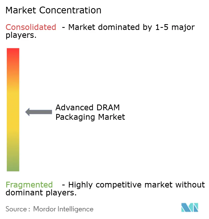
The advanced DRAM packaging market is moderately concentrated at the high end and much more fragmented in standard memory packaging. Samsung Electronics, SK hynix, and Micron remain the core memory OEMs with the strongest positions in qualified HBM-related packaging flows. Their advantage comes from vertical integration across memory design, stacking, testing, and quality control, which is especially valuable in yield-sensitive TSV programs. At the same time, a wider field of OSATs and module specialists competes across standard memory formats, semi-advanced packaging, and overflow demand in the advanced DRAM packaging market. This creates a two-speed competitive structure where technical leadership is concentrated, but broader revenue participation is dispersed.
Strategic moves in 2025 and 2026 showed how competitors are responding to that structure. ASE introduced FOCoS-Bridge with TSV to lower resistance and inductance in AI and HPC packages, which signaled that OSATs are investing in proprietary packaging IP rather than only processing overflow demand. Amkor expanded its Arizona site in 2026, strengthening its position in localized high-volume advanced packaging. SK hynix also moved ahead with its Cheongju packaging investment, which underscored how memory leaders are still scaling captive capability for HBM and next-generation stack development.
The advanced DRAM packaging market therefore remains open enough for OSAT expansion, but not open enough to dilute the leadership of the top memory companies in the most demanding categories. Smaller players such as JCET Group, ChipMOS Technologies, Hana Micron, and Tianshui Huatian Technology remain more active where capital requirements and qualification timelines are less extreme. White space is strongest in automotive and edge AI programs, where long approval cycles and multi-source preferences can favor suppliers outside the main HBM race. Even so, the most advanced tiers of the advanced DRAM packaging market still reward scale, process maturity, and deep customer co-design relationships far more than low-cost assembly alone.
Advanced DRAM Packaging Industry Leaders
-
Samsung Electronics Co., Ltd.
-
SK hynix Inc.
-
Micron Technology, Inc.
-
Taiwan Semiconductor Manufacturing Company Limited
-
Advanced Semiconductor Engineering, Inc.
- *Disclaimer: Major Players sorted in no particular order
Advanced DRAM Packaging Market Companies Covered in this Report
- Samsung Electronics Co., Ltd.
- SK hynix Inc.
- Micron Technology, Inc.
- Taiwan Semiconductor Manufacturing Company Limited
- Advanced Semiconductor Engineering, Inc.
- Amkor Technology, Inc.
- Powertech Technology Inc.
- Jiangsu Changjiang Electronics Technology Co., Ltd.
- King Yuan Electronics Co., Ltd.
- Siliconware Precision Industries Co., Ltd.
- TongFu Microelectronics Co., Ltd.
- Hana Micron Inc.
- ChipMOS TECHNOLOGIES INC.
- Tianshui Huatian Technology Co., Ltd.
- Fujitsu Limited
- Intel Corporation
- Kioxia Corporation
- Tokyo Electron Limited
- United Microelectronics Corporation
- JCET Group Co., Ltd.
Recent Industry Developments in Advanced DRAM Packaging Market
- May 2026: Samsung Electronics shipped the first industry samples of 12-layer HBM4E, featuring 48 GB capacity, 3.6 TB/s per-stack bandwidth, and a 16% energy efficiency improvement versus HBM4; the product uses Samsung's 1c DRAM process and a 4 nm logic base die from Samsung Foundry, and follows HBM4 commercial shipments that began in February 2026.
- April 2026: Samsung Electronics placed orders for approximately 20 EUV lithography systems from ASML, valued at over KRW 10 trillion (USD 7.4 billion), for deployment at the Pyeongtaek P5 Phase 1 cleanroom targeted for early 2027; the equipment directly supports 1c DRAM and HBM4 capacity expansion.
- March 2026: SK hynix disclosed a regulatory filing to purchase more than 30 EUV scanner units from ASML for approximately KRW 11.95 trillion (USD 8.8 billion), with delivery targeted by December 2027, to support 1c DRAM production for HBM4 at the M15X Cheongju facility and the upcoming Yongin Cluster.
- February 2026: SK hynix approved an additional KRW 21.61 trillion (USD 15.1 billion) investment for Phases 2-6 of its Yongin Semiconductor Cluster first fab, bringing total committed investment for the first fab to approximately KRW 31 trillion (USD 21.5 billion), anchoring 1c DRAM and HBM production plans through 2030.
Global Advanced DRAM Packaging Market Report Scope
The Advanced DRAM Packaging Market refers to the global market for semiconductor packaging technologies, materials, and assembly services used specifically in the manufacturing of DRAM devices.
The Advanced DRAM Packaging Market Report is Segmented by Packaging Type (Standard DRAM Packaging, Package-on-Package (PoP) for DRAM-Based Memory Modules, Flip-Chip DRAM Packaging, Wafer-Level Chip Scale Packaging (WLCSP), and Others (3D Stacked DRAM Packaging, High Bandwidth Memory (HBM) Packaging)), Integration Technology (Wire Bonding, Flip-Chip Bonding, Through-Silicon Via (TSV) Based Stacking, Die Stacking, Wafer-to-Wafer Bonding, and Others (Die-to-Wafer Bonding, Hybrid Bonding)), Substrate Type (Organic Substrate, Leadframe Package, Silicon Interposer / TSV-Based Interconnect, Advanced Build-Up Substrate, and Others (Fan-Out Wafer-Level Packaging, Emerging Advanced Substrates)), Ecosystem Channel (DRAM Manufacturers, OSATs, Advanced Packaging Foundries, and Module Assemblers) End Use (Servers and Data Centers, PCs and Laptops, Smartphones and Tablets, Consumer Electronics, and Others (Graphics and Gaming Devices, Automotive Electronics)), and Geography (North America, Europe, Asia-Pacific, Rest of World). The Market Forecasts are Provided in Terms of Value (USD).
Segmentation Overview
| Standard DRAM Packaging |
| Package-on-Package (PoP) for DRAM-Based Memory Modules |
| Flip-Chip DRAM Packaging |
| Wafer-Level Chip Scale Packaging (WLCSP) |
| Other Packaging Types (3D Stacked DRAM Packaging, High Bandwidth Memory (HBM) Packaging) |
| Wire Bonding |
| Flip-Chip Bonding |
| Through-Silicon Via (TSV) Based Stacking |
| Die Stacking |
| Wafer-to-Wafer Bonding |
| Other Integration Technologies (Die-to-Wafer Bonding, Hybrid Bonding) |
| Organic Substrate |
| Leadframe Package |
| Silicon Interposer / TSV-Based Interconnect |
| Advanced Build-Up Substrate |
| Other Substrate / Interposer Types (Fan-Out Wafer-Level Packaging, Emerging Advanced Substrates) |
| DRAM Manufacturers |
| OSATs |
| Advanced Packaging Foundries |
| Module Assemblers |
| Servers and Data Centers |
| PCs and Laptops |
| Smartphones and Tablets |
| Consumer Electronics |
| Other End Uses (Graphics and Gaming Devices, Automotive Electronics) |
| North America | |
| Europe | |
| Asia-Pacific | China |
| Japan | |
| South Korea | |
| Taiwan | |
| Rest of Asia-Pacific | |
| Rest of the World |
| By Packaging Type | Standard DRAM Packaging | |
| Package-on-Package (PoP) for DRAM-Based Memory Modules | ||
| Flip-Chip DRAM Packaging | ||
| Wafer-Level Chip Scale Packaging (WLCSP) | ||
| Other Packaging Types (3D Stacked DRAM Packaging, High Bandwidth Memory (HBM) Packaging) | ||
| By Integration Technology | Wire Bonding | |
| Flip-Chip Bonding | ||
| Through-Silicon Via (TSV) Based Stacking | ||
| Die Stacking | ||
| Wafer-to-Wafer Bonding | ||
| Other Integration Technologies (Die-to-Wafer Bonding, Hybrid Bonding) | ||
| By Substrate / Interposer Type | Organic Substrate | |
| Leadframe Package | ||
| Silicon Interposer / TSV-Based Interconnect | ||
| Advanced Build-Up Substrate | ||
| Other Substrate / Interposer Types (Fan-Out Wafer-Level Packaging, Emerging Advanced Substrates) | ||
| By Ecosystem Channel | DRAM Manufacturers | |
| OSATs | ||
| Advanced Packaging Foundries | ||
| Module Assemblers | ||
| By End Use | Servers and Data Centers | |
| PCs and Laptops | ||
| Smartphones and Tablets | ||
| Consumer Electronics | ||
| Other End Uses (Graphics and Gaming Devices, Automotive Electronics) | ||
| By Geography | North America | |
| Europe | ||
| Asia-Pacific | China | |
| Japan | ||
| South Korea | ||
| Taiwan | ||
| Rest of Asia-Pacific | ||
| Rest of the World | ||
Key Questions Answered in the Report
What is the advanced DRAM packaging market size through 2031?
The advanced DRAM packaging market size was USD 13.84 billion in 2025 and is forecast to reach USD 17.35 billion by 2031 at a 3.86% CAGR over 2026-2031.
Which segment leads advanced DRAM packaging by packaging type?
Standard DRAM packaging led with 49.67% of revenue in 2025, showing that conventional DDR-related formats still anchor shipment volume even as HBM attracts most strategic investment.
Which integration technology is growing the fastest in advanced DRAM packaging?
TSV-based stacking is projected to grow at a 4.52% CAGR through 2031 because HBM adoption in AI accelerators depends on dense vertical interconnect structures.
Why are servers and data centers so important for this space?
Servers and data centers held 35.78% of revenue in 2025 and are also the fastest-growing end use at 4.52% CAGR, driven by rising HBM content in AI training and inference systems.
Which region dominates advanced DRAM packaging today?
Asia-Pacific led with an 85.43% share in 2025 because the region concentrates DRAM fabrication, OSAT infrastructure, and advanced substrate supply.
What is the main challenge limiting faster expansion?
The biggest constraints are high capital intensity, yield loss risk in multi-die and TSV stacks, and tight substrate availability, which keep the market structurally supply limited.