5G Semiconductor Silicon Wafer Market Size and Share
Market Overview
| Study Period | 2020 - 2031 |
|---|---|
| Market Volume (2026) | 382.95 Million Square Inches |
| Market Volume (2031) | 689.02 Million Square Inches |
| Growth Rate (2026 - 2031) | 12.47% CAGR |
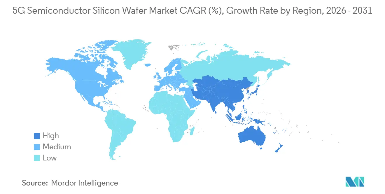
| Fastest Growing Market | Asia Pacific |
| Largest Market | Asia Pacific |
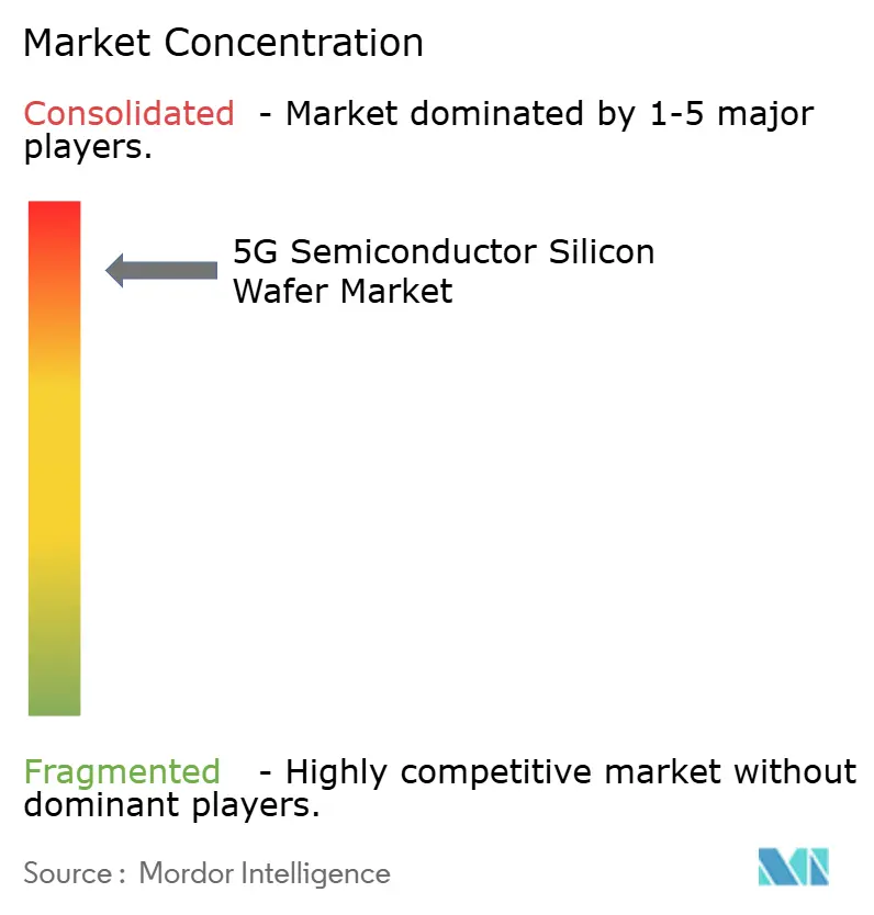
| Market Concentration | High |
Major Players *Disclaimer: Major Players sorted in no particular order Image © Mordor Intelligence. Reuse requires attribution under CC BY 4.0. | |
5G Semiconductor Silicon Wafer Market Analysis by Mordor Intelligence
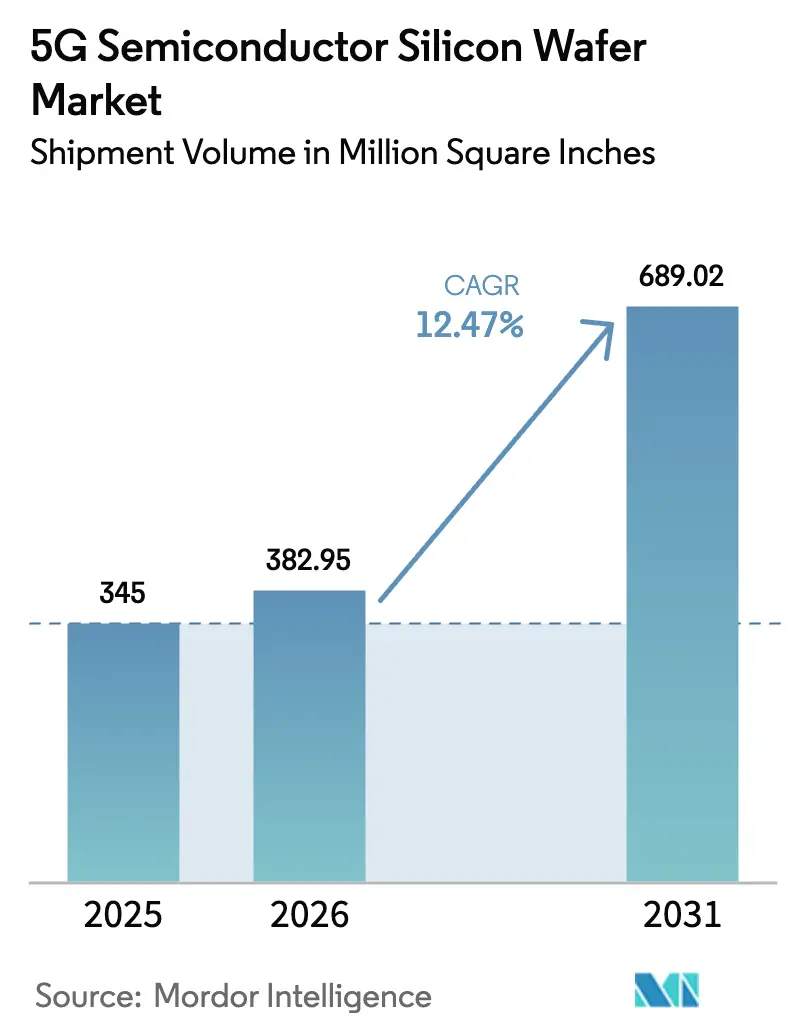
The 5G semiconductor silicon wafer market size is expected to grow from 345 million square inches in 2025 to 382.95 million square inches in 2026, and is forecast to reach 689.02 million square inches by 2031, at a 12.47% CAGR over 2026-2031. Sub-7-nanometer migration across smartphones, densification of urban 5G infrastructure, and sustained conversion to 300-millimeter substrates remain the structural growth engines for the 5G semiconductor silicon wafer market. Strong procurement from Asia-Pacific handset makers secures long-term foundry output, while North American and European onshoring programs diversify geographic supply without displacing the region’s dominance. Tight substrate availability enables the top five wafer makers to push annual price escalators, and recent consolidation, such as Doosan’s purchase of SK Siltron, intensifies the negotiating leverage of incumbents. Environmental restrictions on ultra-pure water usage and polysilicon price swings temper margin expansion but have not derailed capex programs that underpin the 5G semiconductor silicon wafer market’s growth trajectory.
Key Report Takeaways
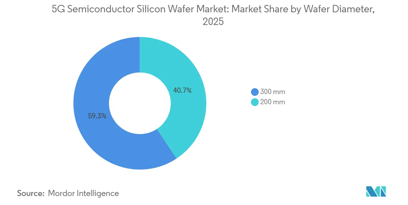
- By wafer diameter, the 300 mm segment captured 59.32% of the 5G semiconductor silicon wafer market share in 2025, and it is advancing at a 13.23% CAGR through 2031.
- By technology node, mainstream nodes (10nm-28nm) accounted for 43.78% of the market share in 2025; advanced node (Below 7nm) posted the fastest growth at a 13.73% CAGR over 2026-2031.
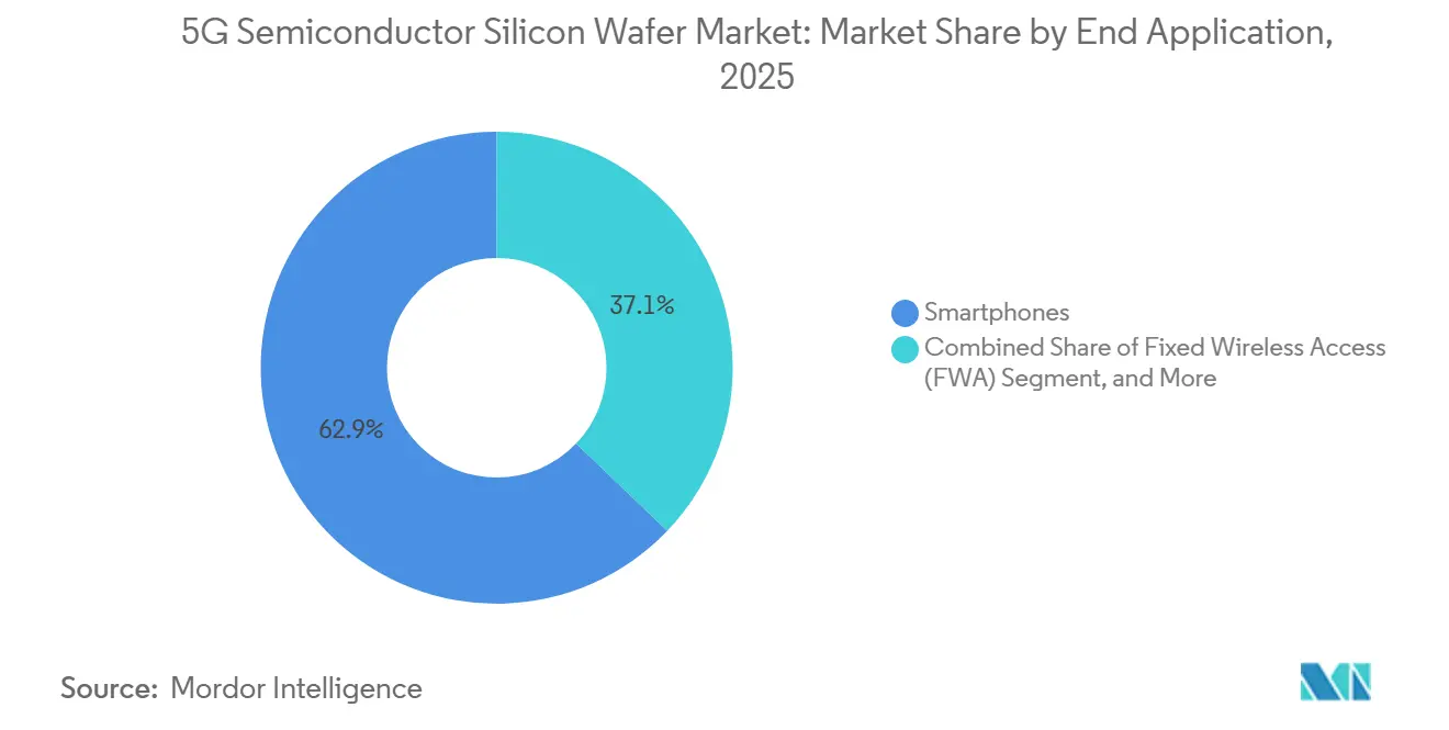
- By end application, smartphones dominated with 62.86% of the market share in 2025, whereas fixed wireless access equipment is the fastest-growing segment, with a 13.46% CAGR to 2031.
- By geography, Asia-Pacific commanded 72.61% of the market share in 2025 and also leads expansion at a 13.83% CAGR through 2031.
Note: Market size and forecast figures in this report are generated using Mordor Intelligence’s proprietary estimation framework, updated with the latest available data and insights as of January 2026.
Global 5G Semiconductor Silicon Wafer Market Trends and Insights
Drivers Impact Analysis*
| Driver | (~) % Impact on CAGR Forecast | Geographic Relevance | Impact Timeline |
|---|---|---|---|
| Surging Mobile Data Traffic from 5G Smartphones | +2.8% | Global, with peak intensity in Asia-Pacific and North America | Short term (≤ 2 years) |
| Rapid Deployment of 5G Telecom Infrastructure | +2.5% | Asia-Pacific core, spillover to Middle East and Africa | Medium term (2-4 years) |
| Increasing Demand for Advanced Node Chips in 5G Devices | +2.2% | Taiwan, South Korea, United States (foundry hubs) | Medium term (2-4 years) |
| Adoption of Silicon Wafer Thinning for 5G mmWave Antenna Integration | +1.5% | North America and Europe (mmWave spectrum allocations) | Long term (≥ 4 years) |
| Growth of Private 5G Networks in Industrial Automation | +1.3% | Germany, United States, Japan (manufacturing corridors) | Long term (≥ 4 years) |
| Government Incentives for Localized Wafer Fabrication in Emerging Economies | +1.2% | India, Vietnam, Mexico (emerging semiconductor hubs) | Long term (≥ 4 years) |
| Source: Mordor Intelligence | |||
Surging Mobile Data Traffic from 5G Smartphones
Global 5G handset shipments reached 1.2 billion in 2024 and are forecast to hit 1.5 billion by 2026, each premium device relying on sub-7 nanometer dies that consume materially larger wafer area. Flagship processors, such as Apple’s A18 Pro with 19 billion transistors, demand silicon flatness below 0.3 micrometers to avoid EUV patterning defects.[1]Apple Inc., “A18 Pro Chip Architecture,” APPLE.COM Foundries pre-book 300 millimeter capacity up to a year ahead, pushing substrate list prices 12%-15% higher year-on-year. Because a single sub-20 nanometer particle can kill an entire advanced die, customers increasingly shift to epitaxial-quality wafers with <0.01 defects per cm², locking in premium contracts for the 5G semiconductor silicon wafer market.
Rapid Deployment of 5G Telecom Infrastructure
China installed 4.2 million 5G base stations by December 2024 and targets 5 million by end-2025, retaining mature-node demand for RF front-ends while digital baseband moves to 7 nanometers. European operators accelerated small-cell rollouts using Ericsson’s RAN Compute systems that integrate 7 nanometer ASSPs.[2]Ericsson, “RAN Compute Portfolio for 5G Networks,” ERICSSON.COM The densification wave multiplies required sites per square kilometer, lifting mixed-node wafer demand spanning 180 nanometers to 7 nanometers. Suppliers serving the 5G semiconductor silicon wafer market, therefore, schedule overlapping 200 millimeter and 300 millimeter production runs to hedge node volatility.
Increasing Demand for Advanced Node Chips in 5G Devices
TSMC ramped 3 nanometer production to 100 000 wafer starts per month by mid-2025, allocating roughly 60% to smartphone SoCs. Samsung Foundry qualified its 3 nanometer gate-all-around flow in early 2025, but initial yield gaps caused substrate lead times to spike from 12 weeks to 18 weeks. Intel’s 18A node enters high volume in 2026 with backside power delivery that further tightens flatness and contamination specs. These migrations expand die sizes, lifting wafer area per handset by 15%-20% and supporting double-digit growth for the 5G semiconductor silicon wafer market.
Adoption of Silicon Wafer Thinning for 5G mmWave Antenna Integration
Millimeter-wave deployments in the United States and parts of Europe force handset OEMs to thin silicon from 775 micrometers to 50-100 micrometers so phased-array antennas sit within 2 millimeters of the RF die.[3]IEEE, “Thin-Wafer Processing for mmWave Antenna Integration,” IEEEXPLORE.IEEE.ORG Skyworks and Qorvo shifted roughly one-quarter of their mmWave product lines to thin-wafer silicon-on-insulator during 2024-2025. Thinning raises breakage risk and processing costs by 30%, but enables 70% antenna efficiency at 28 GHz. Specialty thin-wafer capacity thus becomes a differentiated pocket of the 5G semiconductor silicon wafer market.
Restraints Impact Analysis*
| Restraint | (~) % Impact on CAGR Forecast | Geographic Relevance | Impact Timeline |
|---|---|---|---|
| High Capital Expenditure for 300 mm Wafer Fabs | -0.8% | Global, acute in emerging economies without subsidy programs | Medium term (2-4 years) |
| Supply Chain Disruptions of Semiconductor Grade Polysilicon | -0.6% | Global, with acute exposure in China and Southeast Asia | Short term (≤ 2 years) |
| Yield Challenges at Below 7nm Nodes for RF Front-End ICs | -0.5% | Taiwan, South Korea, United States (advanced foundry locations) | Medium term (2-4 years) |
| Environmental Regulations Limiting Ultra-Pure Water Usage in Wafer Production | -0.3% | Europe, California, Taiwan (water-stressed regions) | Long term (≥ 4 years) |
| Source: Mordor Intelligence | |||
High Capital Expenditure for 300 mm Wafer Fabs
Building a greenfield 300 millimeter plant costs USD 10 billion-USD 20 billion, keeping new entry rare and reinforcing the oligopoly that underpins pricing power. GlobalWafers’ USD 7.5 billion Texas project received USD 1.5 billion in U.S. grants, yet still faces a five-year ramp before revenue begins. SUMCO elected to close a legacy 200 millimeter line rather than reinvest, signaling that even incumbents exit sub-scale assets when payback periods lengthen. Resulting capacity staging in 50,000-wafer-per-month increments limits supply elasticity for the 5G semiconductor silicon wafer market.
Supply Chain Disruptions of Semiconductor Grade Polysilicon
Six vendors control 85% of 11-nines polysilicon and solar-sector swings sent prices from USD 35/kg in early 2024 to USD 22/kg by mid-2025.[4]Wacker Chemie AG, “Polysilicon Market Dynamics,” WACKER.COM Smaller wafer makers lacking long-term contracts endured abrupt margin erosion, prompting two Japanese exits between 2022 and 2024. Entity-List restrictions complicate Chinese access to Western polysilicon, driving defect-density upticks and forcing wafer firms to carry as much as 120 days of inventory. Volatility in this critical input remains a latent drag on the 5G semiconductor silicon wafer market.
*Our forecasts treat driver/restraint impacts as directional, not additive. The impact forecasts reflect baseline growth, mix effects, and variable interactions.
Segment Analysis
By Wafer Diameter: Larger Substrates Capture Economies Of Scale
The 300 millimeter category held 59.32% of the market share in 2025 and benefits from a 13.23% CAGR, cementing its primacy through 2031. Each 300-millimeter wafer yields roughly 2.4× the die count of a 200-millimeter wafer, translating to 30%-35% lower unit fabrication cost once depreciation is absorbed. Leading fabs in Arizona, Pyeongtaek, and Ireland process only this diameter, ensuring locked-in baseline demand. The 5G semiconductor silicon wafer market size for 300 millimeter substrates will therefore scale faster than any other diameter set.
Although 200 millimeters remains indispensable for legacy RF, power, and MEMS, capital plans heavily favor 300 millimeter lines capable of ultra-thin grinding for chip-on-wafer-on-substrate packaging. Suppliers able to guarantee warp-free thinning below 50 micrometers capture premium contracts, while second-tier producers focus on stabilizing 200-micrometer service for automotive and industrial buyers. This bifurcation secures long-run growth and cushions cyclicality within the broader 5G semiconductor silicon wafer market.


By Technology Node: Advanced Nodes Outpace Mainstream Despite Complexity
Mainstream Node (10nm-28nm) accounted for 43.78% of the market share in 2025, owing to RF, PMIC, and mixed-signal designs that reward mature-node economics. Gross margins often exceed leading-edge logic because specialty process tweaks limit competitive supply. Consequently, the 5G semiconductor silicon wafer market share for mainstream nodes remains large even as die counts per product shrink.
Advanced Node (Below 7nm), however, registers a 13.73% CAGR through 2031, fueled by application processors and AI accelerators in premium smartphones. TSMC and Samsung allocate the bulk of their 3-nanometer capacity to handset silicon, driving substrate flatness, oxygen precipitate control, and contamination thresholds that only the top two wafer makers can reliably meet. As advanced-node uptake widens to fixed wireless access and edge AI, the 5G semiconductor silicon wafer market size tied to nodes below 7 nanometers will steadily expand.
By End Application: Smartphones Dominate, FWA Surges
Smartphones accounted for 62.86% of the market share in 2025, with each flagship handset embedding six to eight discrete 5G chips that double silicon area versus 4G designs. Apple and Samsung device refresh cycles now integrate larger AI blocks, lifting wafer area per unit by an additional 15%-20%. This content enrichment sustains absolute volume even as handset shipments plateau, locking in the smartphone anchor for the 5G semiconductor silicon wafer market.
Fixed wireless access is recording the fastest expansion, with a 13.46% CAGR, driven by rural broadband objectives in the United States, Europe, and parts of Asia. Platforms such as Qualcomm’s Snapdragon X75 unify millimeter-wave and sub-6 gigahertz radios on a single die, compressing bill of materials yet drawing steady volumes from 12 nanometer and 4 nanometer foundry lines. Infrastructure and industrial segments contribute balanced mid-teens growth, collectively dampening cyclical exposure for the 5G semiconductor silicon wafer market.

Geography Analysis
Asia-Pacific controlled 72.61% of the 5G semiconductor silicon wafer market in 2025 and expands at 13.83% CAGR through 2031. China’s 4.2 million macro base stations and Taiwan’s foundry cluster together generate unrivaled demand pools, while Japanese wafer suppliers command more than half of global 300 millimeter output. Regional policy, notably Beijing’s localization mandates and Tokyo’s advanced packaging subsidies, further anchors capacity and reinforces the region’s leadership position.
North America captures strategic mindshare through the U.S. CHIPS and Science Act, which subsidizes fabs in Texas, Arizona, New York, and Ohio. Once fully online by 2028, these sites will consume roughly 30-35 million square inches annually about 10% global share securing domestic supply for defense and critical infrastructure without materially eroding Asia’s volume lead. Canada and Mexico accelerate complimentary back-end and mature-node investments, rounding out a continental ecosystem that supports the 5G semiconductor silicon wafer market.
Europe’s Chips Act channels EUR 43 billion (USD 47 billion) into new capacity, lifting regional wafer demand from 8% in 2025 toward an expected 12%-14% by 2030 once sites in Magdeburg and Dresden ramp. South America and the Middle East and Africa jointly remain below 3% share, with growth tied to automotive electrification in Brazil and data-center deployments in the United Arab Emirates. These smaller regions nonetheless widen the global footprint of the 5G semiconductor silicon wafer market.

Competitive Landscape
The market is concentrated with suppliers such as Shin-Etsu Chemical, SUMCO, GlobalWafers, Siltronic, SK Siltron, and others in the 5G semiconductor silicon wafer market. Doosan’s USD 3.2 billion purchase of SK Siltron has tightened the South Korean supply. Meanwhile, Siltronic’s expansion in Singapore and GlobalWafers’ facility in Texas have diversified the regional footprint without reducing market concentration.
Patent data reveal sustained investment in the mitigation of defects and nanotopography. Shin-Etsu holds 47 active filings on oxygen precipitation control, while SUMCO leads in epitaxial-layer uniformity techniques. This intellectual-property moat, along with USD 10 billion-plus greenfield price tags, discourages new entrants and reinforces the high-barrier structure of the 5G semiconductor silicon wafer market.
Specialty niches do provide openings. Wafer Works and Gritek emphasize silicon-on-insulator and reclaim services for mature nodes, securing 30%-40% price premiums at lower volumes. Chinese challengers Zhejiang Jinruihong and Ferrotec’s Shanghai arm expand 200-millimeter lines but still face multi-year qualification cycles with tier-one customers. As heterogeneous integration accelerates, suppliers that master sub-50 micrometer thinning, through-silicon vias, and zero-delamination bonding will hold an outsized share of emerging value pools within the 5G semiconductor silicon wafer market.
5G Semiconductor Silicon Wafer Industry Leaders
Shin-Etsu Chemical Co., Ltd.
SUMCO Corporation
GlobalWafers Co., Ltd.
Siltronic AG
SK Siltron Co., Ltd.
- *Disclaimer: Major Players sorted in no particular order

Recent Industry Developments
- January 2026: Micron Technology broke ground on a USD 24 billion NAND flash fab in Singapore, set to consume 15 million square inches of 300 millimeter wafers annually upon 2028 ramp.
- December 2025: Doosan Corporation finalized its USD 3.2 billion acquisition of SK Siltron, including silicon-carbide assets in Michigan.
- October 2025: TSMC’s Kumamoto fab achieved 28 nanometer qualification ahead of schedule, securing wafer supply from nearby SUMCO plants.
- September 2025: GlobalFoundries invested USD 1.5 billion to lift Malta, New York capacity by 25 000 wafer starts per month of 12 nanometer FinFET.


Global 5G Semiconductor Silicon Wafer Market Report Scope
The 5G Semiconductor Silicon Wafer Market refers to the market for silicon wafers specifically designed and manufactured for use in 5G-related applications, including smartphones, telecom infrastructure, fixed wireless access, and industrial 5G.
The 5G Semiconductor Silicon Wafer Market Report is Segmented by Wafer Diameter (300 mm, and 200 mm), Technology Node (Advanced Node, Mainstream Node, and Mature Node), End Application (Smartphones, Telecom Infrastructure, Fixed Wireless Access, and Industrial 5G), and Geography (North America, Europe, Asia-Pacific, South America, and Middle East and Africa). The Market Forecasts are Provided in Terms of Volume (Square Inches).
| 300 mm |
| 200 mm |
| Advanced Node (Below 7nm) |
| Mainstream Node (10nm-28nm) |
| Mature Node (Above 28nm) |
| Smartphones |
| Telecom Infrastructure (Macro / Small Cells) |
| Fixed Wireless Access (FWA) |
| Industrial 5G |
| North America | United States |
| Canada | |
| Mexico | |
| Europe | Germany |
| United Kingdom | |
| France | |
| Rest of Europe | |
| Asia-Pacific | China |
| Japan | |
| India | |
| South Korea | |
| Taiwan | |
| Rest of Asia-Pacific | |
| South America | |
| Middle East and Africa |
| By Wafer Diameter | 300 mm | |
| 200 mm | ||
| By Technology Node | Advanced Node (Below 7nm) | |
| Mainstream Node (10nm-28nm) | ||
| Mature Node (Above 28nm) | ||
| By End Application | Smartphones | |
| Telecom Infrastructure (Macro / Small Cells) | ||
| Fixed Wireless Access (FWA) | ||
| Industrial 5G | ||
| By Geography | North America | United States |
| Canada | ||
| Mexico | ||
| Europe | Germany | |
| United Kingdom | ||
| France | ||
| Rest of Europe | ||
| Asia-Pacific | China | |
| Japan | ||
| India | ||
| South Korea | ||
| Taiwan | ||
| Rest of Asia-Pacific | ||
| South America | ||
| Middle East and Africa | ||


Key Questions Answered in the Report
What is the projected 5G semiconductor silicon wafer market size by 2031?
It is forecast to reach 689.02 million square inches by 2031.
Which wafer diameter segment leads the 5G semiconductor silicon wafer market?
The 300 millimeter segment led with 59.32% of the market share in 2025 and will maintain leadership through 2031.
Why is Asia-Pacific dominant in the 5G semiconductor silicon wafer space?
The region hosts the largest foundry clusters and 5G base-station deployments, together driving more than 70% of global wafer demand.
How will U.S. onshoring affect wafer supply?
New fabs in Texas, Arizona, and Ohio will raise North American consumption to roughly 10% of global volume by 2028, improving regional resilience without eroding Asia's lead.
Which application shows the fastest wafer demand growth?
Fixed wireless access equipment records the highest growth at 13.46% CAGR to 2031 as operators extend broadband
Page last updated on:


