Market Size of Thin Wafer Processing and Dicing Equipment Industry
| Study Period | 2019 - 2029 |
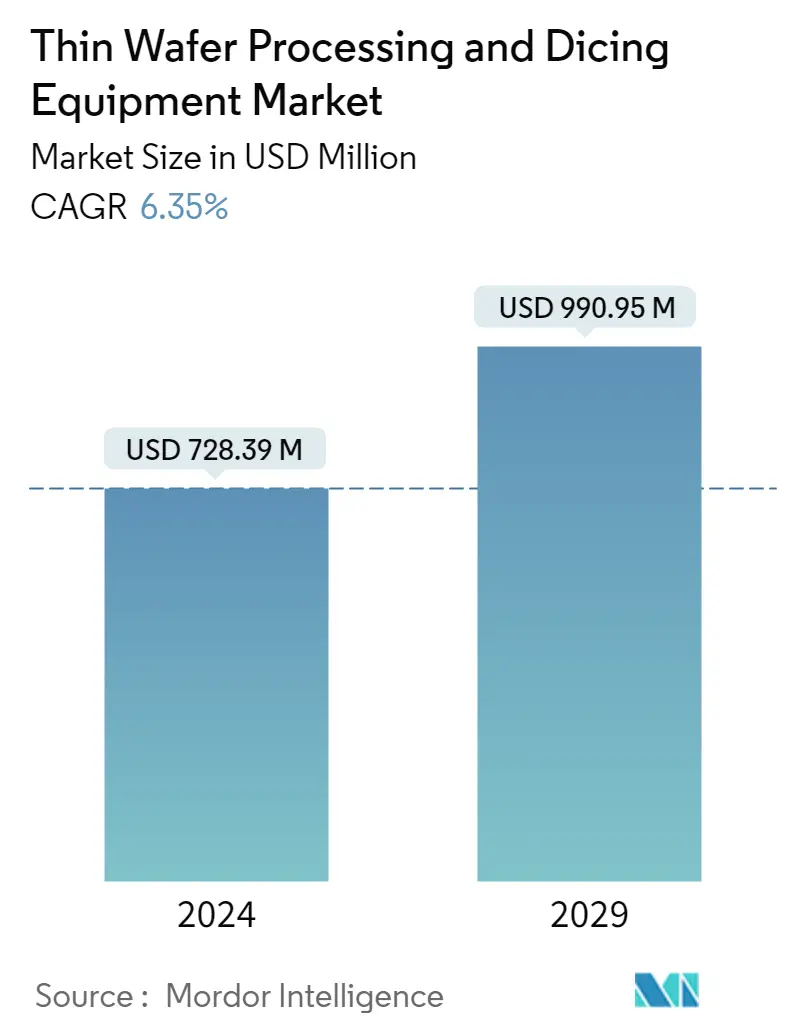
| Market Size (2024) | USD 728.39 Million |
| Market Size (2029) | USD 990.95 Million |
| CAGR (2024 - 2029) | 6.35 % |
| Fastest Growing Market | Asia Pacific |
| Largest Market | Asia Pacific |
Major Players
*Disclaimer: Major Players sorted in no particular order |
Need a report that reflects how COVID-19 has impacted this market and its growth?
Thin Wafer Processing & Dicing Equipment Market Analysis
The Thin Wafer Processing and Dicing Equipment Market size is estimated at USD 728.39 million in 2024, and is expected to reach USD 990.95 million by 2029, growing at a CAGR of 6.35% during the forecast period (2024-2029).
The increasing efforts to make electronic packaging highly resourceful due to the enormous demand for electronic components owing to amplified usage have made electronic packaging useful in a myriad of applications. These factors are driving the growth of the semiconductor and IC packaging market.
- One of the major factors expected to boost the demand for thin wafer processing and dicing equipment in the coming years is the growing demand for three-dimensional integrated circuits, which are widely used in miniature semiconductor devices such as memory cards, smartphones, and smart cards, and various computing devices. Three-dimensional circuits are becoming more popular in multiple space-constrained applications, such as portable consumer electronics, sensors, MEMS, and industrial products because they improve overall product performance in terms of speed, durability, low power consumption, and lightweight memory.
- The expanding use of server and data center systems across various enterprises and industries, due to the widespread availability of low-cost cloud computing solutions, is likely to fuel demand for logic devices like microprocessors and digital signal processors. In addition, as the number of IoT-enabled linked devices grows, the utilization of microprocessors also increases. Thin wafers are increasingly employed in these devices to enable effective temperature management and enhance performance. All of these reasons are assisting in expanding the logic device market.
- Silicon wafers have long been used as a fabrication platform in microelectronics and MEMS. The silicon-on-insulator substrate is a unique variation of the standard silicon wafer. Two silicon wafers are glued together using a bond layer of silicon dioxide with a thickness of about 1-2 m to make these wafers. One silicon wafer gets flattened down to 10-50 m in thickness. The application will determine the exact thickness of the coating.
- The cost of building state-of-the-art thin wafer foundries has increased exponentially, which puts pressure on the industry. This is where the number of semiconductor manufacturers was consolidated in recent times. Performance boosts are slowing down, making specialized thin wafers increasingly attractive. The design decisions that enable thin wafers to be universal may be sub-optimal for some computing tasks.
- Due to the global slowdown in demand in the industrial and automotive electronics sectors that the COVID-19 pandemic has worsened, manufacturers operating in the market have registered a decline in orders for Thin Wafer semiconductors.
