Metasurface Imaging Systems Market Size and Share
Market Overview
| Study Period | 2020 - 2031 |
|---|---|
| Market Size (2026) | USD 118.31 Million |
| Market Size (2031) | USD 442.17 Million |
| Growth Rate (2026 - 2031) | 30.17 % |
| Fastest Growing Market | Asia-Pacific |
| Largest Market | North America |
| Market Concentration | Medium |
Major Players *Disclaimer: Major Players sorted in no particular order Image © Mordor Intelligence. Reuse requires attribution under CC BY 4.0. | |
Metasurface Imaging Systems Market Analysis by Mordor Intelligence
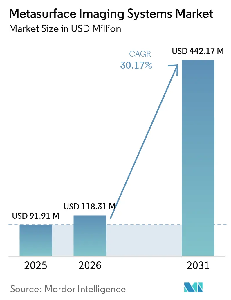
The Metasurface imaging systems market size is projected to expand from USD 91.91 million in 2025 and USD 118.31 million in 2026 to USD 442.17 million by 2031, registering a CAGR of 30.17% between 2026 to 2031. The Metasurface imaging systems market is moving from technical demonstrations toward volume production as wafer-scale fabrication becomes more practical. Flat optical elements can replace larger lens stacks and reduce the space required by camera and sensing modules. This supports adoption where device height, power use, and reliability are important, including consumer devices, vehicles, and industrial equipment. Semiconductor manufacturing also gives suppliers a route to improve yields and reduce unit costs as production volumes rise. High design, mask, and packaging costs remain a constraint for specialized programs that cannot spread fixed costs across large order volumes.
Key Report Takeaways
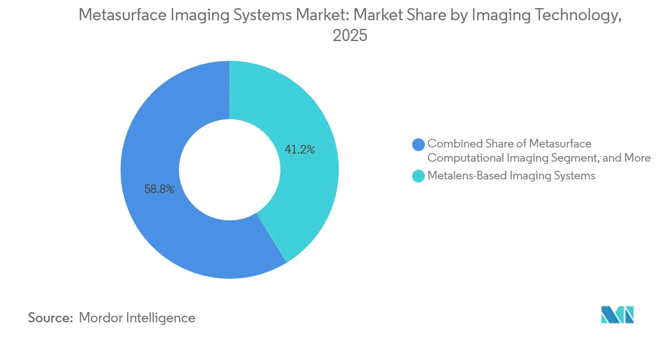
- By imaging technology, metalens-based imaging systems held 41.23% of the Metasurface imaging systems market in 2025, while metasurface computational imaging is projected to expand at a 31.46% CAGR through 2031.
- By imaging modality, 2D imaging accounted for 35.67% of revenue in 2025, while computational and 4D imaging are projected to expand at a 31.73% CAGR through 2031.
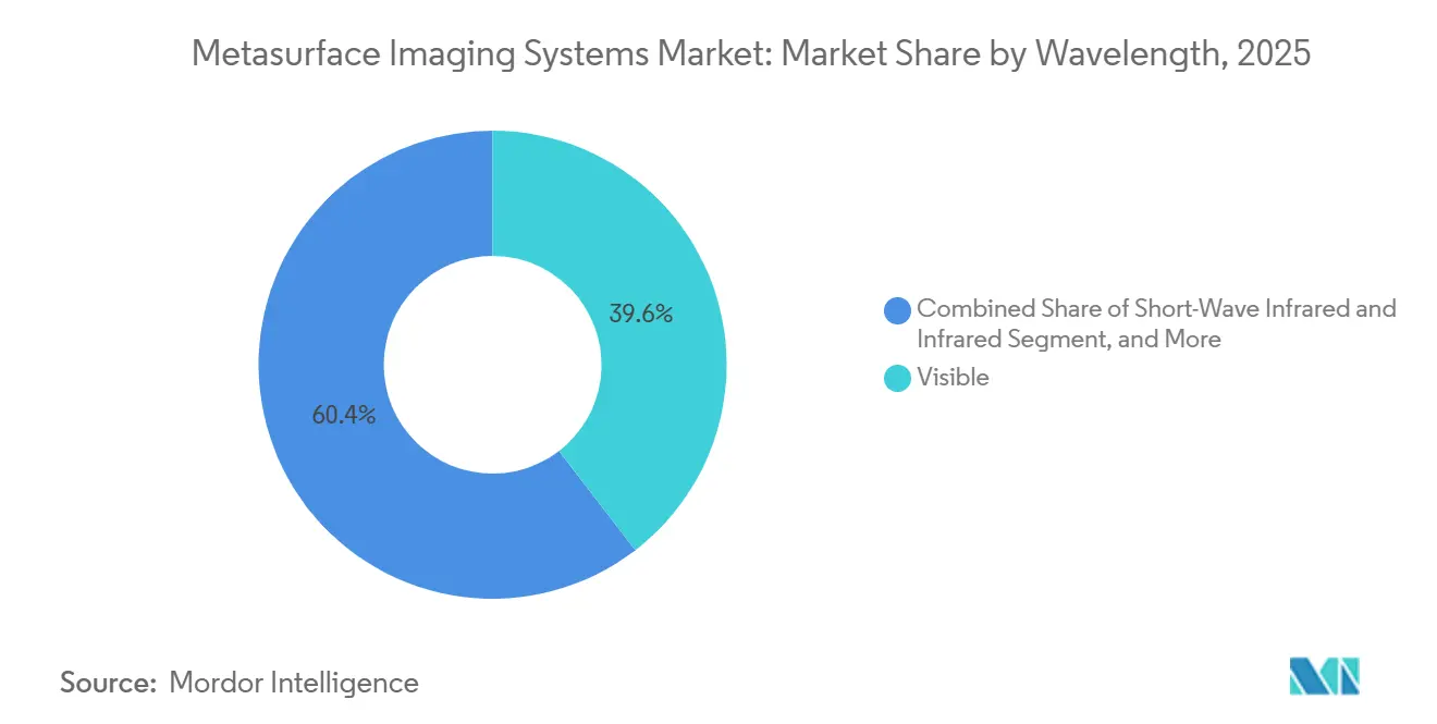
- By wavelength, visible light accounted for 39.56% of revenue in 2025, while terahertz imaging is projected to expand at a 31.67% CAGR through 2031.
- By application, consumer electronics held 24.56% revenue share in 2025, while automotive and LiDAR are projected to expand at a 31.58% CAGR through 2031.
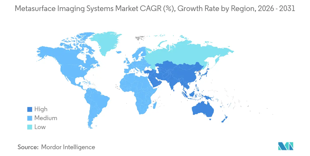
- By geography, North America held 36.42% of the Metasurface imaging systems market share in 2025, while Asia-Pacific is projected to expand at a 32.26% CAGR through 2031.
Note: Market size and forecast figures in this report are generated using Mordor Intelligence’s proprietary estimation framework, updated with the latest available data and insights as of January 2026.
Global Metasurface Imaging Systems Market Trends and Insights
Drivers Impact Analysis*
| Driver | (~) % Impact on CAGR Forecast | Geographic Relevance | Impact Timeline |
|---|---|---|---|
| Wafer-Scale Meta-Optics Commercialization | +8.2% | Global, led by North America and Asia-Pacific | Short term (≤ 2 years) |
| Smaller, Lower-Power Imaging Modules | +6.5% | Global, especially Asia-Pacific and North America | Short term (≤ 2 years) |
| Automotive LiDAR and Machine-Vision Adoption | +5.8% | North America, Europe, and Asia-Pacific | Medium term (2-4 years) |
| Polarization and Spectral Imaging Growth | +4.2% | North America and Europe, with Asia-Pacific adoption | Medium term (2-4 years) |
| CMOS-Compatible Manufacturing Standardization | +3.5% | Global | Medium term (2-4 years) |
| New Information From Computational Meta-Optics | +2.8% | North America, Europe, and Asia-Pacific | Long term (≥ 4 years) |
| Source: Mordor Intelligence | |||
Wafer-Scale Meta-Optics Commercialization Changes Unit Economics
Wafer-scale production is becoming a central requirement for the Metasurface imaging systems market because it can move flat optics from limited prototypes into repeatable manufacturing. A 2026 study reported a roll-to-roll nanoimprint process that produced 300 metalenses per second from 200-meter film arrays with 80nm feature resolution. The reported throughput was 2 orders of magnitude higher than conventional nanoimprint lithography methods. A wafer-level meta-aspheric lens also achieved a 101.5° field of view within a 3.39mm track length and 0.02 cm³ volume. These developments show how refractive and metasurface elements can be integrated on a single wafer for compact near-infrared imaging. An Advanced Materials study in 2025 also demonstrated full 8-inch wafer-scale titanium dioxide metalens imprinting, with nearly 1,000 4mm-diameter lenses on each wafer.
Smaller, Lower-Power Imaging Modules Reshape Device Design
Demand for thinner, lower-power modules supports the Metasurface imaging systems market across devices with constrained space and mechanical complexity. Direct sensor integration can reduce the need for larger lens assemblies and autofocus mechanisms. This matters for wearable electronics, edge devices, medical instruments, and automotive cameras that need a compact optical path. Passive wavefront coding can also reduce reliance on moving components that increase power consumption and introduce potential failure points. MetaOptics shipped metalens smartphones and AI smart glasses for customer evaluation in June 2026, indicating that this form-factor objective has reached OEM assessment programs
Automotive LiDAR and Machine Vision Extend Use in Safety Programs
Automotive LiDAR and machine vision provide an important qualification path for the Metasurface imaging systems market. Lumotive combined its LM10 Light Control Metasurface with an Adaps Photonics dTOF sensor in April 2026 for a solid-state 180° LiDAR platform operating at 30 frames per second with a 50-meter range in rain and low-visibility conditions.[1]Lumotive, “Lumotive Creates World’s First 2D Photonic Beamforming Semiconductor,” Lumotive, lumotive.com. The company also demonstrated a 2D photonic beamforming semiconductor in March 2026 that steered light in 2 axes without moving parts. The architecture was designed for operation at 905nm, 1,310nm, and 1,550nm. Stable performance across automotive temperature ranges is important because vehicle suppliers need traceable and reliable sensor systems.
Polarization and Spectral Imaging Broaden Addressable Uses
Polarization and spectral sensing expand the Metasurface imaging systems market beyond conventional color imaging. Tunoptix introduced a compact hyperspectral platform in 2025 that was smaller than 1 cm³ and captured more than 30 visible and near-infrared channels with sub-20nm resolution. The study reported 7 times higher image resolution and 4.5 times lower reconstruction error than the preceding reference device. These capabilities allow a flat element to capture information that otherwise requires several filters or optical stages. The resulting systems can support industrial inspection, target recognition, and biomedical imaging where contrast or material information is needed.
Restraints Impact Analysis*
| Restraint | (~) % Impact on CAGR Forecast | Geographic Relevance | Impact Timeline |
|---|---|---|---|
| High Nonrecurring Engineering and Packaging Costs | -3.8% | Global | Short term (≤ 2 years) |
| Software and Calibration for Optical Aberration Correction | -3.2% | Global | Short term (≤ 2 years) |
| Foundry Access and Intellectual Property Concentration | -2.1% | Global, particularly Asia-Pacific emerging markets | Medium term (2-4 years) |
| Limited Harsh-Environment Qualification Data | -1.5% | Automotive-focused regions, Europe and North America | Long term (≥ 4 years) |
| Source: Mordor Intelligence | |||
High Nonrecurring Engineering and Packaging Costs Limit Mid-Volume Adoption
High engineering and packaging expenses limit access to the Metasurface imaging systems market for mid-volume industrial and medical programs. Custom mask sets and sub-micron active alignment equipment impose fixed costs that are difficult to recoup on specialized products. Cost parity with conventional refractive elements requires annual volumes in the millions of units. Catalog products can spread mask costs among several customers, but they may offer less scope for unusual wavelengths or apertures. Multi-project wafer programs could lower entry costs, although broad adoption by foundries remained limited in 2026.
Optical Aberration Correction Extends Integration Timelines
Optical aberration correction remains a practical challenge for the Metasurface imaging systems market when systems operate under broadband illumination. Wavelength-dependent phase dispersion can require computational processing or more complex achromatic designs to produce accurate color images. Research on 2025 achromatic metalenses showed that inverse design of meta-atom dimensions requires specialized computation during optical development. OEMs may therefore need signal-processing capability as well as a suitable optical component. An ACS Nano review identified a lack of standardized evaluation methods and constrained design methodology among the major commercialization barriers beyond fabrication yield. Qualification periods, which normally last 18-24 months, can be extended by 6-12 months when wavefront correction algorithms are included in the hardware program.
*Our forecasts treat driver/restraint impacts as directional, not additive. The impact forecasts reflect baseline growth, mix effects, and variable interactions.
Segment Analysis
By Imaging Technology: Metalenses Hold an Early Commercial Lead
Metalens-based imaging systems accounted for 41.23% of the Metasurface imaging systems market in 2025. Their lead reflected early commercial use in time-of-flight sensors and structured-light systems. Repeated orders for depth sensors, biometric modules, and industrial range finders gave producers operating experience in volume fabrication. That learning supported improvements in yield and unit cost. The Metasurface imaging systems market also includes holographic and polarimetric imaging systems.
Metasurface computational imaging is projected to grow at a 31.46% CAGR through 2031. The category combines optical encoding with reconstruction software to collect depth, polarization, and spectral information from a single capture. Metalenz launched Polar 3D in February 2026 to create on-device 3D facial information from one image using shape-from-polarization.[2]Metalenz, “Polar 3D From Metalenz Delivers Relightable Selfies and Realistic Avatars on Device from a Single Image,” Metalenz, metalenz.com. The feature was intended for avatars and edge computing applications in smartphones and laptops. A 2026 preprint also described a compact camera that captured hyperspectral and polarization information in a single snapshot across nearly the entire visible spectrum.



By Imaging Modality: 2D Imaging Leads While Computational and 4D Imaging Advances Fastest
2D imaging held 35.67% of the Metasurface imaging systems market in 2025. Within the Metasurface imaging systems market, the category benefits from the installed base of digital camera sensors and straightforward replacement of refractive lenses in flat imaging configurations. Its immediate value is lower module height rather than a change in the information captured. 3D and depth imaging, hyperspectral imaging, multispectral imaging, and polarimetric imaging held smaller positions. These systems are gaining relevance as detectors become more accessible and edge processing improves.
Computational and 4D imaging is projected to expand at a 31.73% CAGR through 2031. The modality can record several dimensions of optical information without multiplying sensor count. A 2026 infrared meta-sensor demonstrated real-time hyperspectral and polarimetric imaging at 55 frames per second. The reported reconstruction error was 4.5 times lower than that of the previous reference approach. Snapshot collection eliminates the need for repeated exposures that filter wheels and rotating polarizers require.
By Wavelength: Visible Light Leads While Terahertz Supports Inspection
Visible light accounted for 39.56% of the Metasurface imaging systems market in 2025. The Metasurface imaging systems market uses visible wavelengths in consumer cameras, augmented reality displays, and industrial machine vision within the 400-700nm range. Near-infrared was the next major wavelength category because LiDAR and facial recognition systems use 850nm and 940nm bands. Short-wave infrared and infrared systems serve thermal imaging and night-vision needs. Ultraviolet metasurfaces remained mainly in qualification for lithography inspection and biomedical microscopy.
Terahertz imaging is projected to grow at a 31.67% CAGR through 2031. A 2026 study demonstrated pixelated bound-state-in-the-continuum metasurfaces for real-time terahertz imaging and reported 100% binary image reconstruction from a single terahertz pulse. The system also demonstrated refractive-index sensing above 14.39 GHz/RIU. Separate 2026 research integrated vanadium dioxide into a phase-change metasurface that could switch between edge detection and bright-field imaging through software control. This combination is relevant to non-destructive inspection, security screening, and pharmaceutical quality control.
By Application: Consumer Electronics Leads as Automotive and LiDAR Gain Scale
Consumer electronics held 24.56% of the Metasurface imaging systems market share in 2025. Smartphones, tablets, and smart speakers have created volume demand for time-of-flight and biometric sensing modules. A flat metalens can perform the function of a 3-5 element refractive stack at one-tenth of the package height. This design can reduce thermal sensitivity and improve reliability in portable equipment. Kyocera demonstrated a metasurface-based wearable aerial display at CES 2026 that used wavelength-controlled focal-position manipulation for depth perception.
Automotive and LiDAR are projected to expand at a 31.58% CAGR through 2031. Lumotive and E-Photonics introduced LiDAR-metasurface integrated systems for the Saudi Arabian market at LEAP 2025. The companies presented systems with 25-meter and 80-meter range configurations. The application also includes solid-state sensing that avoids the need for mechanical scanning components. Biomedical and life sciences, industrial inspection and metrology, aerospace and defense, and scientific imaging remain lower-volume areas with demanding optical requirements.
Geography Analysis
North America accounted for 36.42% of regional revenue in 2025. The region benefits from foundational intellectual property, defense demand, and venture funding for deep technology companies. Metalenz, Lumotive, and 2Pi Optics show how university research programs have moved toward commercial metasurface platforms. Metalenz confirmed in May 2025 that its Polar ID system had entered smartphone integration trials for anticipated 2026 deployment. The Samsung ISOCELL Vizion 931 sensor served as the stated hardware platform for the program.
Asia-Pacific is projected to grow at a 32.26% CAGR through 2031. China, Japan, South Korea, and Taiwan have consumer electronics and semiconductor manufacturing networks that influence global component costs. Kyocera presented metasurface display optics at CES 2026. MetaOptics began evaluation shipments of metalens smartphone and AI smart-glasses products to customers in Japan and Europe in June 2026. Radiant Opto-Electronics acquired NIL Technology in May 2025, linking European meta-optics capabilities with Asian commercial channels.
Europe has activity in automotive imaging, photonics research, and precision industrial inspection. The Metasurface imaging systems market has regional activity in Germany for automotive programs and in France and the Netherlands for photonics research. The European Innovation Council's OPTIPATH project is developing MEMS-metasurface integration for miniature cameras, communications, and 3D imaging.[3]European Commission, “OPTIPATH,” CORDIS, europa.eu. NIL Technology and SINTEF are participants in the project.

Competitive Landscape
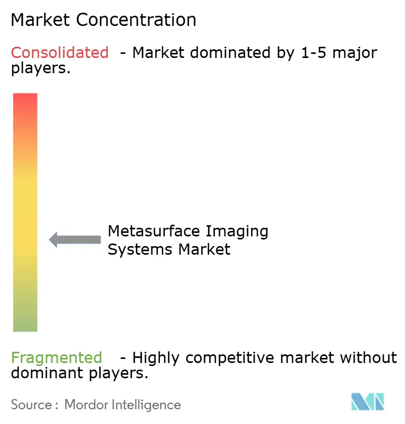
The Metasurface imaging systems market is moderately fragmented. Intellectual property-focused specialists operate alongside semiconductor manufacturers that can scale production through licensing. Metalenz holds rights to foundational Harvard metasurface patents and reports a portfolio of more than 150 active applications and issued patents. Its licensing relationship with STMicroelectronics gives it recurring intellectual property revenue as production volumes increase. STMicroelectronics has shipped more than 140 million metasurface optics and FlightSense modules using Metalenz intellectual property since 2022.
Lumotive competes through programmable optical semiconductors and LiDAR reference designs. The company reported total Series B proceeds of USD 59 million in July 2025 and planned data-center optical switching products for the end of 2026. NIL Technology focuses on nanoimprint manufacturing and its metaCamera product line. Tunoptix focuses on computational hyperspectral platforms, while 2Pi Optics develops CMOS-compatible flat optics for AI infrastructure and automotive sensing.
Across the Metasurface imaging systems market, competition depends on access to fabrication, optical performance, software capabilities, and qualified modules. Leading suppliers are increasingly pairing optical hardware with a specific system function. Metalenz launched Polar 3D in February 2026 to link polarimetric hardware with on-device 3D facial data and avatar applications.[4]Metalenz, “STMicroelectronics and Metalenz Sign a New License Agreement to Accelerate Metasurface Optics Adoption,” Metalenz, metalenz.com. Lumotive demonstrated its 2D photonic beamforming semiconductor in March 2026 for electronically steered solid-state optical systems.
Metasurface Imaging Systems Industry Leaders
Metalenz, Inc.
STMicroelectronics N.V.
NIL Technology ApS
MetaOptics Technologies Pte. Ltd.
Lumotive, Inc.
- *Disclaimer: Major Players sorted in no particular order

Recent Industry Developments
- July 2026: MetaOptics Technologies and Elsoft Research Berhad announced a partnership to co-develop 12-inch large-format metalens laser writers and automatic testers covering visible 425-630nm, near-infrared 740-940nm, and short-wave infrared 1,245-1,310nm wavelength ranges. The partnership targets high-volume metalens fabrication and test equipment infrastructure.
- April 2026: Lumotive's LM10 Light Control Metasurface combined with the Adaps Photonics ADS6311 Hawk dTOF sensor delivered a solid-state 180° LiDAR platform at 30 frames per second with 50-meter range performance under rain and low-visibility conditions. A commercially available reference design is accessible to LiDAR module manufacturers.
- March 2026: Lumotive demonstrated a 2D photonic beamforming semiconductor chip built on its Light Control Metasurface architecture. The chip enabled real-time light steering across 2 spatial axes without moving parts at 905nm, 1,310nm, and 1,550nm, with commercial optical switch products for data-center interconnect targeted by the end of 2026.
- February 2026: Metalenz launched Polar 3D, extending its Polar ID face-authentication platform into digital presence by using monocular shape-from-polarization to generate on-device 3D facial data from a single image. The platform enables relightable selfies, photorealistic avatars, and virtual try-on applications without cloud computation or multi-angle scans.


Global Metasurface Imaging Systems Market Report Scope
Metasurface imaging systems use engineered, ultrathin surfaces with nanoscale structures to manipulate electromagnetic waves and improve imaging performance. These systems enable compact, lightweight, and high-resolution imaging solutions across applications such as medical imaging, consumer electronics, automotive sensing, and defense.
The Metasurface Imaging Systems Market Report is Segmented by Imaging Technology (Metalens-Based Imaging Systems, Metasurface Holographic Imaging, Metasurface Computational Imaging, Metasurface Polarimetric Imaging, and Other Imaging Technologies), Imaging Modality (2D Imaging, 3D/Depth Imaging, Hyperspectral/Multispectral Imaging, Polarimetric Imaging, Computational/4D Imaging, and Other Imaging Modalities), Wavelength (Ultraviolet, Visible, Near Infrared, Short-Wave Infrared and Infrared, and Terahertz), Application (Consumer Electronics, Biomedical and Life Sciences, Industrial Inspection and Metrology, Automotive and LiDAR, Aerospace and Defense, AR/VR and Wearable Imaging, Scientific and Research Imaging, and Other Applications), and Geography (North America, South America, Europe, Asia-Pacific, Middle East, and Africa). The Market Forecasts are Provided in Terms of Value (USD).
| Metalens-Based Imaging Systems |
| Metasurface Holographic Imaging |
| Metasurface Computational Imaging |
| Metasurface Polarimetric Imaging |
| Other Imaging Technologies |
| 2D Imaging |
| 3D / Depth Imaging |
| Hyperspectral / Multispectral Imaging |
| Polarimetric Imaging |
| Computational / 4D Imaging |
| Other Imaging Modalities |
| Ultraviolet |
| Visible |
| Near Infrared |
| Short-Wave Infrared and Infrared |
| Terahertz |
| Consumer Electronics |
| Biomedical and Life Sciences |
| Industrial Inspection and Metrology |
| Automotive and LiDAR |
| Aerospace and Defense |
| AR/VR and Wearable Imaging |
| Scientific and Research Imaging |
| Other Applications |
| North America | United States |
| Canada | |
| Mexico | |
| South America | Brazil |
| Argentina | |
| Chile | |
| Rest of South America | |
| Europe | Germany |
| United Kingdom | |
| France | |
| Italy | |
| Spain | |
| Rest of Europe | |
| Asia-Pacific | China |
| Japan | |
| India | |
| South Korea | |
| Australia | |
| Rest of Asia-Pacific | |
| Middle East | United Arab Emirates |
| Saudi Arabia | |
| Qatar | |
| Rest of Middle East | |
| Africa | South Africa |
| Egypt | |
| Nigeria | |
| Rest of Africa |
| By Imaging Technology | Metalens-Based Imaging Systems | |
| Metasurface Holographic Imaging | ||
| Metasurface Computational Imaging | ||
| Metasurface Polarimetric Imaging | ||
| Other Imaging Technologies | ||
| By Imaging Modality | 2D Imaging | |
| 3D / Depth Imaging | ||
| Hyperspectral / Multispectral Imaging | ||
| Polarimetric Imaging | ||
| Computational / 4D Imaging | ||
| Other Imaging Modalities | ||
| By Wavelength | Ultraviolet | |
| Visible | ||
| Near Infrared | ||
| Short-Wave Infrared and Infrared | ||
| Terahertz | ||
| By Application | Consumer Electronics | |
| Biomedical and Life Sciences | ||
| Industrial Inspection and Metrology | ||
| Automotive and LiDAR | ||
| Aerospace and Defense | ||
| AR/VR and Wearable Imaging | ||
| Scientific and Research Imaging | ||
| Other Applications | ||
| By Geography | North America | United States |
| Canada | ||
| Mexico | ||
| South America | Brazil | |
| Argentina | ||
| Chile | ||
| Rest of South America | ||
| Europe | Germany | |
| United Kingdom | ||
| France | ||
| Italy | ||
| Spain | ||
| Rest of Europe | ||
| Asia-Pacific | China | |
| Japan | ||
| India | ||
| South Korea | ||
| Australia | ||
| Rest of Asia-Pacific | ||
| Middle East | United Arab Emirates | |
| Saudi Arabia | ||
| Qatar | ||
| Rest of Middle East | ||
| Africa | South Africa | |
| Egypt | ||
| Nigeria | ||
| Rest of Africa | ||


Key Questions Answered in the Report
What is the size of the metasurface imaging systems market?
The metasurface imaging systems market size is projected to reach USD 442.17 million by 2031 from USD 118.31 million in 2026, at a 30.17% CAGR. The outlook reflects the shift from limited optical prototypes toward higher-volume wafer-scale production.
What is driving demand for metasurface imaging systems?
Wafer-scale production, compact low-power modules, automotive LiDAR, and polarization and spectral sensing support adoption. These requirements align with smaller optical paths and integrated sensing in devices.
Which imaging technology led in 2025?
Metalens-based imaging systems led with 41.23% revenue share in 2025, supported by time-of-flight and structured-light applications. The category benefits from early manufacturing experience and repeat-volume use cases.
Which application is expected to grow fastest through 2031?
Automotive and LiDAR is projected to record the fastest application CAGR at 31.58% through 2031. Solid-state light steering supports the application’s requirement for compact sensor systems.
Which region leads and which is growing fastest?
North America held 36.42% revenue share in 2025, while Asia-Pacific is projected to grow at a 32.26% CAGR through 2031. The Metasurface imaging systems market benefits from Asia-Pacific’s semiconductor and consumer electronics supply chains.
Page last updated on: