Market Trends of Global Wafer Processing and Assembly Equipment Industry
This section covers the major market trends shaping the Wafer Processing & Assembly Equipment Market according to our research experts:
Thin Film Deposition is One of the Factor Driving the Market
- The Chemical Vapor Deposition (CVD) technology is commonly employed in the fabrication of semiconductors and thin films. The expansion of the CVD equipment market is primarily driven by increasing demand for microelectronics-based consumer items, which is resulting in quicker growth of the semiconductor, LED, and storage device industries, as well as severe limits on the use of Cr6 for electroplating.
- In January 2022, ThermVac Inc., a Korean manufacturer of special vacuum furnaces, continues to respond to the needs of domestic and international clients by developing process technology and design and manufacturing technology for CVD equipment that can be used at temperatures ranging from 900°C to 2,400°C. This corresponds to the growing demand for high-temperature heat-resistant CVD components in high-tech industries like semiconductors, solar power, mobile phones, aerospace, and defense.
- The linear sputtering equipment is used in applications like solar energy, display, Data storage, semiconductor, and many more. For instance, in December 2021, Bosch started the volume production of Sic-based power semiconductors supplying automotive manufacturers worldwide. To meet the increasing demand for such semiconductors, an extra 10,764 square feet were already added to the clean-room space at the Bosch wafer fab in Reutlingen in 2021. Another 32,292 square feet will be added by the end of 2023. Such an increase in the production of semiconductors will drive the studied market.
- The advancements in the regional automotive industry are expected to create significant opportunities for market growth. For instance, Dubai recently launched a campaign to have 42,000 EVs on the streets of Emirates by 2030. The sputtering equipment is used in the coating of Drive train bearings and components as the increase in the developments of EV vehicles will significantly drive the studied market.
- Sputtered thin films are increasingly being used in biomedical applications. An example is a cylindrical magnetron sputtering to deposit protective coatings on batches of medical stents. Nano-films are widely employed in electronics, textiles, pharmaceuticals, ceramics, and various other applications. Fabrics coated with Nanofilm are often created by chemical vapor deposition, sol-gel technique, and magnetron sputtering. The magnetron sputtering method, for example, offers the benefits of controlled film thickness, high purity, high speed and low temperature, excellent adhesion, ease of operation, and environmental friendliness, among others.
Understand The Key Trends Shaping This Market
Download Sample
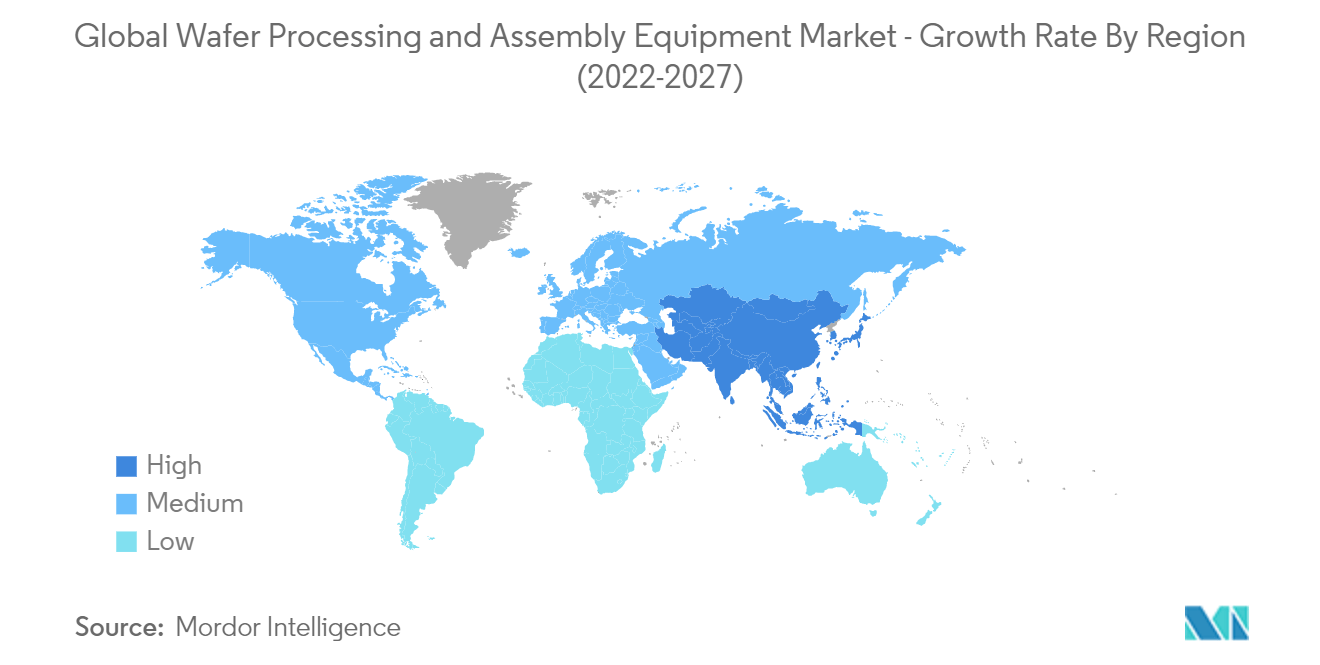
Asia Pacific Holds the Major Share of the Market
- Asia-Pacific has the world's fastest-growing semiconductor market. Many vendors are setting up production facilities in the region in response to strong demand for smartphones and other consumer electronics gadgets from nations including China, the Republic of Korea, and Singapore.
- The companies are expanding their presence in the region by starting new projects to cater to the wide need of the customer. For instance, in September 2021, UTAC Holding, Ltd. added state-of-the-art plasma dicing and multi-project wafer (MPW) capabilities to a range of advanced semiconductor manufacturing solutions. Plasma dicing narrows the scribe line width between chips and increases the number of chips per wafer. Also, it provides "nearly perfect" cutting quality with no chips or cracks, which is a clear advantage over traditional mechanical sawing processes that lead to chronic sidewall quality issues.
- Further public agencies and private companies are investing in new products and research & development facilities. For instance, In September 2021, China's largest contract chipmaker Semiconductor Manufacturing International Corp (SMIC) announced the company's agreement with the Lin-Gang Special area-part of Shanghai's free trade zone. This agreement enables SMIC to establish a new foundry with a monthly planned capacity of 100,000 12-inch wafers. Also, in March 2021, the company announced an investment of USD 2.35 billion in coordination with the Shenzhen government for a manufacturing facility to produce 28nanometre (nm) and above integrated circuits with a monthly capacity of 40,000 12-inch wafers.
- Similarly, in October 2021, the Government of New South Wales is aware that the global semiconductor industry lacks Australia's major players and plans a new center to improve the feasibility of critical jobs in this sector. The hub, the Semiconductor Sector Service Bureau (S3B), will be based in Sydney's Tech Central and be funded by the state government. Further, Chief Scientist and Engineer Office, after researching the national semiconductor scene, mentioned there are currently no major Australian companies with semiconductor design or semiconductor development as their core business. The new hub leverages the country's wafer processing and dicing equipment market.
- The demand for stealth dicing equipment is growing as TSV (Through Silicon Via) technology becomes more prevalent for low-power, high-performance devices such as mobile phones and other wireless and networking devices. As TSV can package 2.5/3D for the applications listed above, the equipment is useful for TSV Assembly/Packaging (chip-to-chip and chip-to-wafer assembly with stealth dicing and other processes). In Memory and Logic, a combination of laser dicing and blade dicing is used.
Get Analysis on Important Geographic Markets
Download Sample
