Market Size of Global Wafer Processing and Assembly Equipment Industry
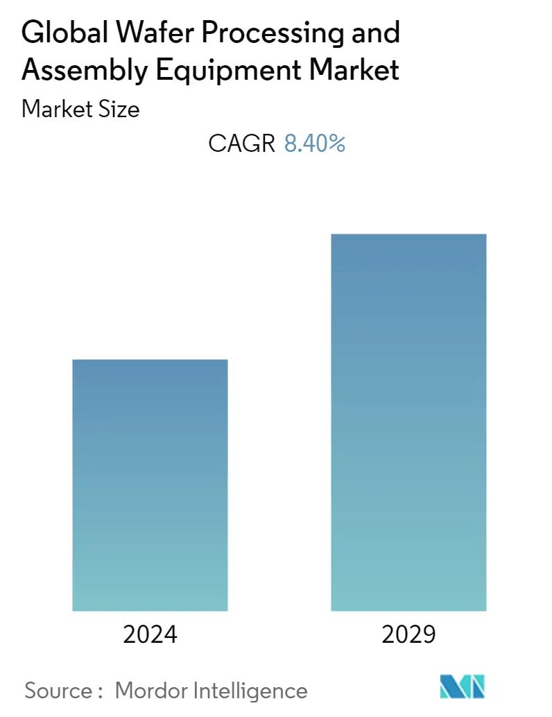
| Study Period | 2019 - 2029 |
| Base Year For Estimation | 2023 |
| CAGR | 8.40 % |
| Fastest Growing Market | Asia-Pacific |
| Largest Market | Asia-Pacific |
| Market Concentration | Medium |
Major Players
*Disclaimer: Major Players sorted in no particular order |
Need a report that reflects how COVID-19 has impacted this market and its growth?
Wafer Processing & Assembly Equipment Market Analysis
The Global Wafer Processing and Assembly Equipment Market is expected to grow at a CAGR of 8.4% during the forecast period of 2022 to 2027. The wafer processing and assembly equipment market is expected to grow in response to rising consumer electronics demand. Customer expectations for improved qualities of new electronic gadgets have risen as demand for electronic products has increased. Several consumer electronics and identity solutions, such as identification tags, smart cards, and others, combine RFIDs with wafers for integrated circuit fabrication. Customers increasingly demand ultra-smooth surfaces and smaller wafers for seamless integration into electronic products.
- According to the Indian Brand Equity Foundation, In 2022, the Indian appliance and consumer electronics (ACE) sector is predicted to grow at a 9% compound annual growth rate (CAGR) to INR 3.15 trillion (USD 48.37 billion). The Indian electronics manufacturing sector is expected to reach USD 300 billion (INR 22.5 lakh crore) by 2024-25. Furthermore, increased consumer electronics device usage and consumption are predicted to fuel semiconductor demand, boosting wafer processing and assembly equipment market revenues throughout the projection period.
- A prominent trend in the wafer processing and assembly equipment industry is the growing demand for miniaturized wafers with higher device performance. Wafers, for example, are flattened down to final thicknesses of tens of micrometers. Most semiconductor wafers used in memory, CIS, and power applications are reduced to 100 µm-200 µm in thickness. In the case of memory devices, further thickness reduction is required due to the need to maximize the memory capacity of single packages, increased data transmission rates, and power consumption fueled mostly by mobile applications. Silicon wafers thicker than 200 µm are used in standard memory devices like 2D NAND/DRAM.
- The government bodies in the different regions are planning to invest in the production of semiconductors, which may create an opportunity for the studied market to grow. For instance, in September 2021, Germany's economy ministry stated that the country is willing to invest EUR 3 billion in the EU's "Important Projects of Common European Interest" initiative, which is one of the EU's primary subsidy tools for stimulating investment and reducing import dependency. The money will be used by the German government to build new semiconductor manufacturing factories. This investment is primarily aimed at reducing dependency on imported semiconductors for future semiconductor needs. Government policies like this will significantly drive the studied market.
- Wafers are subjected to mechanical loads induced by sawing, manual handling, liquid jets, transport systems, and pick and place equipment during the wafer manufacturing cycle. Power semiconductors on the market now are generally made on 200-mm wafers with thicknesses ranging from 50 to 100 µm, although their roadmaps allow for wafers as thin as 1 µm. Mechanical polishing thins the backside of these wafers. Grinding marks, grinding failures resulting in edge chips, star cracks, and comets generated by edge particles caught in the grinding wheel, embedded particles, cleavage lines, and a variety of other faults are all defects caused by the polishing process.
- Furthermore, the global shortage of wafer semiconductors led by the COVID-19 pandemic has encouraged players to focus on increasing production capacity. For instance, Semiconductor Manufacturing International Corp (SMIC) has indulged in aggressive plans to double its production capacity by 2025 by constructing new chip fabrication plants in different cities, including its announcement in September 2021 to establish a new factory in Shanghai's free trade zone.
