
Bottom-Side PCB AOI Systems Market Size and Share
Market Overview
| Study Period | 2020 - 2031 |
|---|---|
| Market Size (2026) | USD 454.82 Million |
| Market Size (2031) | USD 704.01 Million |
| Growth Rate (2026 - 2031) | 9.13 % |
| Fastest Growing Market | Asia-Pacific |
| Largest Market | Asia-Pacific |
| Market Concentration | Medium |
Major Players *Disclaimer: Major Players sorted in no particular order Image © Mordor Intelligence. Reuse requires attribution under CC BY 4.0. | |
Bottom-Side PCB AOI Systems Market Analysis by Mordor Intelligence
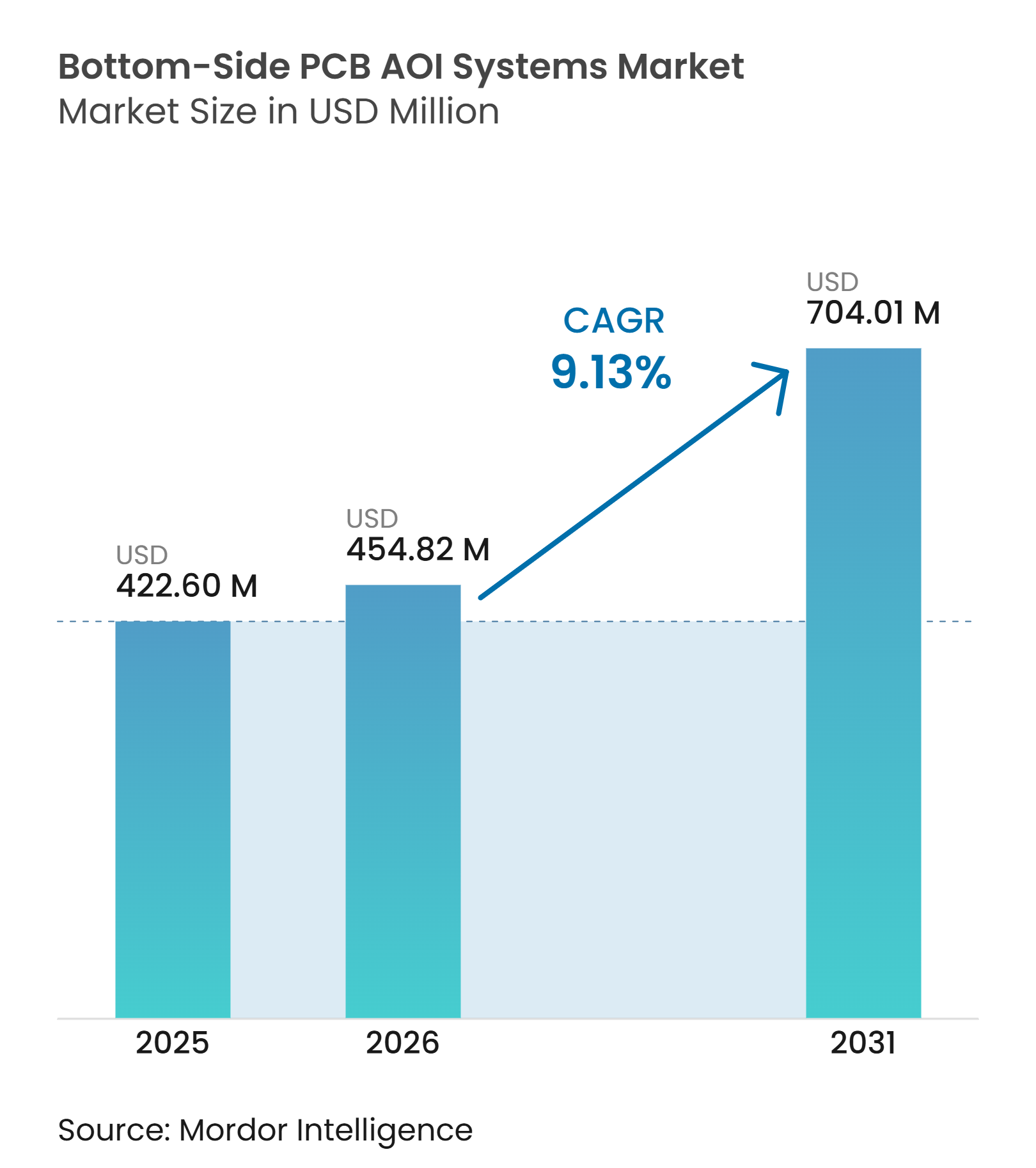
The Bottom-Side PCB AOI Systems Market size was valued at USD 422.60 million in 2025 and estimated to expand from USD 454.82 million in 2026 to reach USD 704.01 million by 2031, at a CAGR of 9.13% during the forecast period (2026-2031). The bottom-side PCB AOI systems market is supported by the wider use of mixed-technology boards that combine surface-mount and through-hole components. These boards require inspection of the underside solder joints after wave or selective soldering. Producers are increasingly using inline systems because board flipping can disrupt throughput in high-volume lines. Quality requirements in automotive, industrial, aerospace, and medical electronics are raising demand for measurement data and traceable inspection records. Suppliers are responding with 3D measurement, AI-assisted programming, and integration of inspection equipment with upstream production tools.
Key Report Takeaways
- By product type, 2D bottom-side AOI systems held 55.27% of the bottom-side PCB AOI systems market share in 2025, while 3D bottom-side AOI systems are projected to expand at a 9.73% CAGR through 2031.
- By the inspection stage, post-wave soldering held 31.43% share in 2025, while post-selective soldering is projected to expand at a 10.12% CAGR through 2031.
- By deployment, inline systems held 62.18% share in 2025, while inspection-island systems are projected to expand at a 9.71% CAGR through 2031.
- By end-user industry, electronics manufacturing held 29.36% share in 2025, while automotive electronics is projected to expand at a 10.68% CAGR through 2031.
- By geography, Asia-Pacific held 44.27% of the bottom-side PCB AOI systems market share in 2025 and is projected to expand at a 10.09% CAGR through 2031.
Note: Market size and forecast figures in this report are generated using Mordor Intelligence’s proprietary estimation framework, updated with the latest available data and insights as of January 2026.
Market Trends and Insights
Drivers Impact Analysis of Bottom-Side PCB AOI Systems Market*
| Driver | (~) % Impact on CAGR Forecast | Geographic Relevance | Impact Timeline |
|---|---|---|---|
| Rising Mixed-Technology PCB Complexity | +2.1% | Global, strongest in China, Japan, South Korea, Germany, and North America | Long term (≥ 4 years) |
| Shift From 2D to 3D Optical Measurement | +1.8% | Global, with higher adoption volume in Asia-Pacific and tighter quality requirements in Europe | Medium term (2-4 years) |
| Industry 4.0 Traceability and Closed-Loop Quality Control | +1.5% | Global, with compliance-led adoption in North America and Europe and throughput-led adoption in Asia-Pacific | Medium term (2-4 years) |
| Zero-Defect Requirements in Automotive and High-Reliability Electronics | +1.3% | North America, Europe, and Asia-Pacific EV powertrain manufacturing | Short term (≤ 2 years) |
| No-Flip Inspection Demand After Wave and Selective Soldering | +0.8% | Global, especially Germany, Japan, and China’s Pearl River Delta | Long term (≥ 4 years) |
| Scarcity of Bottom-Side Defect Training Data Driving AI Investment | +0.5% | Global, with early activity among Asia-Pacific AI-AOI developers | Medium term (2-4 years) |
| Source: Mordor Intelligence | |||
Rising Mixed-Technology PCB Complexity
Mixed-technology PCB designs combine surface-mount parts with through-hole connectors, power inductors, relay blocks, and high-current terminals. Through-hole joints are formed on the underside, so bottom-up optical access is needed to assess barrel fill, solder shape, pin height, and bridging without moving boards to manual inspection. This requirement supports the bottom-side PCB AOI systems market in production lines that use wave and selective soldering. Selective soldering also protects heat-sensitive surface-mount parts from an additional full-board thermal cycle. Its nozzle-based process can produce different joint shapes across components, which increases the value of configurable 3D inspection.
Manufacturers are placing inspection equipment after individual soldering stages rather than relying only on a final check. That arrangement can isolate process variation before it reaches later assembly steps. Bottom-side PCB AOI systems must distinguish between very small passive components and larger high-current connectors on the same board. This range of joint types requires different inspection logic for each component class. Vendors with larger bottom-side defect libraries can improve AI model training and programming automation over time. The bottom-side PCB AOI systems market, therefore, rewards suppliers that can use installed-base inspection data to build stronger application knowledge. Hardware specifications alone are becoming less decisive, as leading 3D platforms deliver comparable measurement capabilities. Algorithm quality, programming automation, and the ability to connect results to production controls have a greater influence on supplier selection. This favors vendors that can support different joint shapes without lengthy manual rule creation.
Shift From 2D To 3D Optical Measurement
Two-dimensional imaging remains useful for visible defects, component presence, polarity, and bridging. However, it cannot provide the same joint height and solder volume information as a 3D system. Automotive power electronics, aerospace boards, and other high-reliability products place greater value on volumetric measurement. The bottom-side PCB AOI systems market is therefore shifting toward platforms that combine image capture with height data. Suppliers are refining structured-light projection, laser triangulation, and multi-color, multi-directional illumination to address bottom-side access constraints.
Bottom-side inspection must operate within a limited clearance between the board and the conveyor system. It must also accommodate flux haze, solder spatter, reflectivity, and shadowing around through-hole fields. The PCB-IND dataset, published in 2026, contains 4,789 industrial AOI images and 5,932 defect instances across 8 categories, providing a dataset for inspection model development. Hybrid systems are gaining relevance because they can use 2D imaging for routine checks and reserve 3D measurement for critical joint areas. This configuration offers wider quality coverage without requiring full-board 3D acquisition for every application. It also lets manufacturers align inspection depth with the risk associated with a component or solder joint. Routine boards can retain fast image-based checks, while critical connections receive volumetric review. The bottom-side PCB AOI systems market benefits from this flexibility, making the transition to 3D more practical for users with mixed board portfolios. Vendors can address cost and cycle-time concerns without reducing the value of height-based inspection.
Industry 4.0 Traceability and Closed-Loop Quality Control
Manufacturers are connecting AOI stations with broader production and quality systems. In these arrangements, inspection output can inform adjustments to solder nozzle dwell time, flux volume, selective-soldering paths, or process temperature. This approach makes closed-loop capability an important consideration alongside inspection speed. Siemens reported sub-3.4 defects per million at its Erlangen PCB facility after using causal AI to relate AOI outputs to upstream process variables.[1] The result illustrates how inspection data can support corrective action before defects affect a larger batch.
Koh Young presented its KPO platform at APEX EXPO 2026 with CUDA-accelerated processing and quantitative True 3D measurement data. The platform is designed to identify solder-paste drift and placement-offset patterns before they affect yield, then support correction at upstream equipment. For bottom-side PCB AOI systems, feedback on selective soldering requires joint-level volume and height information. A 2D image alone cannot provide those measurements. The connected approach also increases the importance of structured records that can be associated with each board and process step. Records can link an observed defect with the nozzle, temperature, flux setting, or placement condition that preceded it. This supports faster root cause analysis and reduces reliance on manual review of inspection images. The bottom-side PCB AOI systems market benefits when AOI is integrated into a connected quality workflow rather than serving as a stand-alone gate. Customers can then consider the system’s contribution to yield, traceability, and process stability together.
Zero-Defect Requirements In Automotive And High-Reliability Electronics
Automotive electronics has stringent inspection requirements because safety-critical boards must meet strict process control and traceability expectations. Battery management, inverters, on-board chargers, and driver-assistance systems use boards with high-current and through-hole connections. These applications support demand for bottom-side PCB AOI systems that can identify visible solder anomalies and retain inspection evidence. IATF 16949-related quality practices require traceability from component lots to final inspection results in automotive PCBA operations. This requirement places greater emphasis on systems that produce structured records rather than on simple pass-or-fail results.
Critical dimensions in automotive assembly are often managed using Cpk targets of at least 1.67. This reinforces the need for repeatable measurement of joint geometry and process variation. Tier 1 suppliers are also passing inspection requirements to Tier 2 and Tier 3 manufacturers. The bottom-side PCB AOI systems market can therefore expand beyond large automotive suppliers into smaller contract manufacturing operations. High-reliability aerospace, defense, and medical applications similarly favor documented inspection coverage for each board. These applications place a greater value on complete records because individual boards can have long service lives and strict acceptance requirements. 3D measurement helps manufacturers assess joint geometry when visual comparison alone is insufficient. The bottom-side PCB AOI systems market also benefits when automotive-quality practices become standard for suppliers serving multiple regulated end uses. This broadens the group of manufacturers that require reliable underside inspection.
Restraints Impact Analysis of Bottom-Side PCB AOI Systems Market*
| Restraint | (~) Impact on CAGR Forecast | Geographic Relevance | Impact Timeline |
|---|---|---|---|
| High Capital Cost and Inline Integration Complexity | -1.7% | Global, especially South America, Middle East and Africa, and Southeast Asian SME assembly clusters | Short term (≤ 2 years) |
| Programming Burden Across High-Mix, Low-Volume Boards | -1.2% | Global, particularly North American and European EMS providers with diverse new-product volumes | Medium term (2-4 years) |
| Flux, Solder Splash, and Contamination on Bottom-Side Optics | -0.7% | Global, especially continuous wave-soldering lines in Asia-Pacific | Long term (≥ 4 years) |
| Occlusion and Shadowing Around Dense Through-Hole Pin Fields | -0.4% | Global, especially industrial and automotive boards with dense connector arrays | Long term (≥ 4 years) |
| Source: Mordor Intelligence | |||
High Capital Cost and Inline Integration Complexity
Premium 3D systems require substantial investment when they include multi-angle imaging and AI inference capabilities. This investment can limit adoption among small and midsize assembly operations. Inline installation also requires conveyor matching, board-support fixtures, manufacturing-execution-system interfaces, and commissioning support. Bottom-side optics need a dedicated clearance zone under the board, which can require custom conveyor sections. These requirements can extend the payback period in regions where contract manufacturers work with lower order values and tighter margins.
The issue is particularly relevant for companies in South America, Southeast Asia, and parts of Eastern Europe. These facilities may recognize the quality benefits but still defer a major line change. Subscription and inspection-as-a-service models are beginning to provide another commercial option. Subscription and inspection-as-a-service models are emerging as another commercial option. These models can improve access for cost-sensitive buyers through per-inspection billing and line-level analytics. The model remains in its early stages outside China and has not yet altered capital allocation patterns across North America or Europe. Smaller manufacturers must still consider operating costs, service coverage, and integration risk before changing their inspection approach. A low initial payment does not eliminate the need for fixtures, data processing, and qualified staff. These factors can lead buyers to keep manual or 2D methods in place for longer than their quality targets would suggest. The bottom-side PCB AOI systems market faces a slower adoption path where production volumes do not justify a dedicated inline installation.
Programming Burden Across High-Mix, Low-Volume Boards
Programming bottom-side inspection is difficult because through-hole component libraries are less standardized than surface-mount libraries. Joint appearance also changes with solder alloy, flux, nozzle geometry, reflectivity, and lighting conditions. High-mix facilities can change products 2 to 5 times a day, making manual program development a material operational burden. DaoAI reported that a legacy rule-based setup can take 2 to 3 hours for each new product introduction and reduce effective line utilization to 70%. Operators may resort to visual inspection while a new program is being stabilized.
AI-based programming tools are intended to reduce this burden. Mycronic stated that its GenI solution reduced new-product-introduction programming time to 10 minutes without requiring prior AOI programming skills. PARMI’s AI Teaching tool programmed a panel with 2,354 components in 2 minutes and 30 seconds by automating component-to-library matching.[2] Adoption is uneven because established facilities must retrain teams and build suitable defect libraries for bottom-side applications. The slower ramp can delay adoption even where capital funding is available. Experienced programmers may be reluctant to replace familiar rule-based practices before they trust an AI-generated program. Facilities also need annotated examples that represent their own solder materials, lighting conditions, and component mix. The bottom-side PCB AOI systems market is affected by this practical transition period because equipment value depends on reliable use after installation. Suppliers that offer application support and faster program validation can reduce this barrier.
*Our forecasts treat driver/restraint impacts as directional, not additive. The impact forecasts reflect baseline growth, mix effects, and variable interactions.
Bottom-Side PCB AOI Systems Market Segment Analysis
By Product Type:
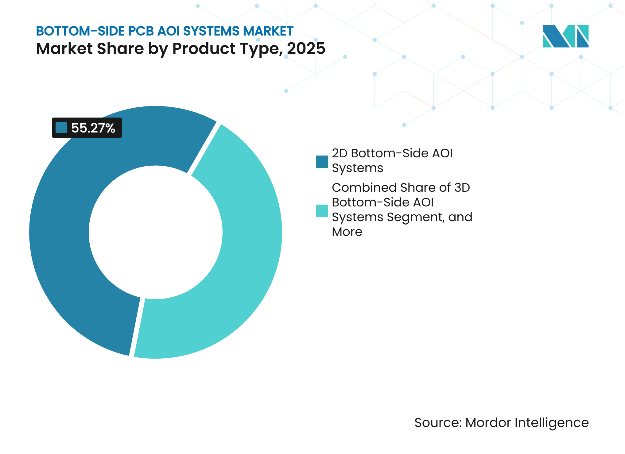
3D Systems Are Expanding In High-Reliability Lines2D bottom-side AOI systems held 55.27% share of the market in 2025. Their position reflects lower cost, faster program setup, and sufficient coverage for many visible through-hole defects. They remain well-suited to consumer electronics, telecommunications equipment, and standard industrial assembly. These environments often prioritize throughput and inspection cost per board. Controlled pin-height variation and standardized solder materials can also reduce the need for detailed height measurement.
3D bottom-side AOI systems are projected to expand at a 9.73% CAGR through 2031. Automotive powertrains and aerospace electronics are moving inspection specifications toward solder volume and pin height measurements. ViTrox launched the V510Ai DST in August 2025, offering simultaneous dual-sided 3D inspection, including bottom-side pin height and solder volume measurements for assemblies with top-side components up to 100 mm. Hybrid systems combine 2D speed for routine checks with 3D measurement at selected joints. They allow industrial users to strengthen coverage without replacing all existing inspection infrastructure or accepting the cycle-time demand of full-board 3D inspection. Structured-light, laser triangulation, and multi-directional lighting methods are being adapted for the restricted geometry beneath a board. The optical design must account for reflectivity from solder surfaces and for residue that can accumulate near the inspection zone. This keeps 2D systems relevant in applications with stable process conditions. It also gives the bottom-side PCB AOI systems market a broader transition path from established 2D equipment to more measurement-intensive systems.


By Inspection Stage:
Post-Selective Soldering Is Advancing RapidlyPost-wave soldering accounted for 31.43% of the bottom-side PCB AOI systems market size in 2025. Its lead reflects the large installed base of wave-soldering equipment in consumer and standard industrial assembly lines, particularly in the Asia-Pacific region. This installed base can support revenue even as selective soldering gains a larger role. Pre-soldering and post-reflow inspection are less consistently associated with the board underside. Their role is expanding on double-sided surface-mount boards that use a secondary reflow pass before through-hole assembly.
Post-selective soldering is projected to expand at a 10.12% CAGR through 2031. Selective soldering limits thermal exposure for sensitive surface-mount components by applying solder through a precision nozzle. Joint shape can vary with nozzle diameter, dwell time, and flux activation, which makes consistent inspection more difficult. Final assembly and rework verification remain important for aerospace and defense boards that require a documented check before shipment. The bottom-side PCB AOI systems market benefits when stations capture joint coordinates, height data, volume estimates, defect classifications, and operator overrides in machine-readable records. Post-selective stations must connect each result to the nozzle, alloy temperature, and flux settings used for that joint. This deeper traceability can make software integration as important as camera and lighting performance. Flexible final-inspection cells also support nonstandard board geometries and different component heights. These needs create demand for systems that can operate across production and rework workflows.
By Deployment:
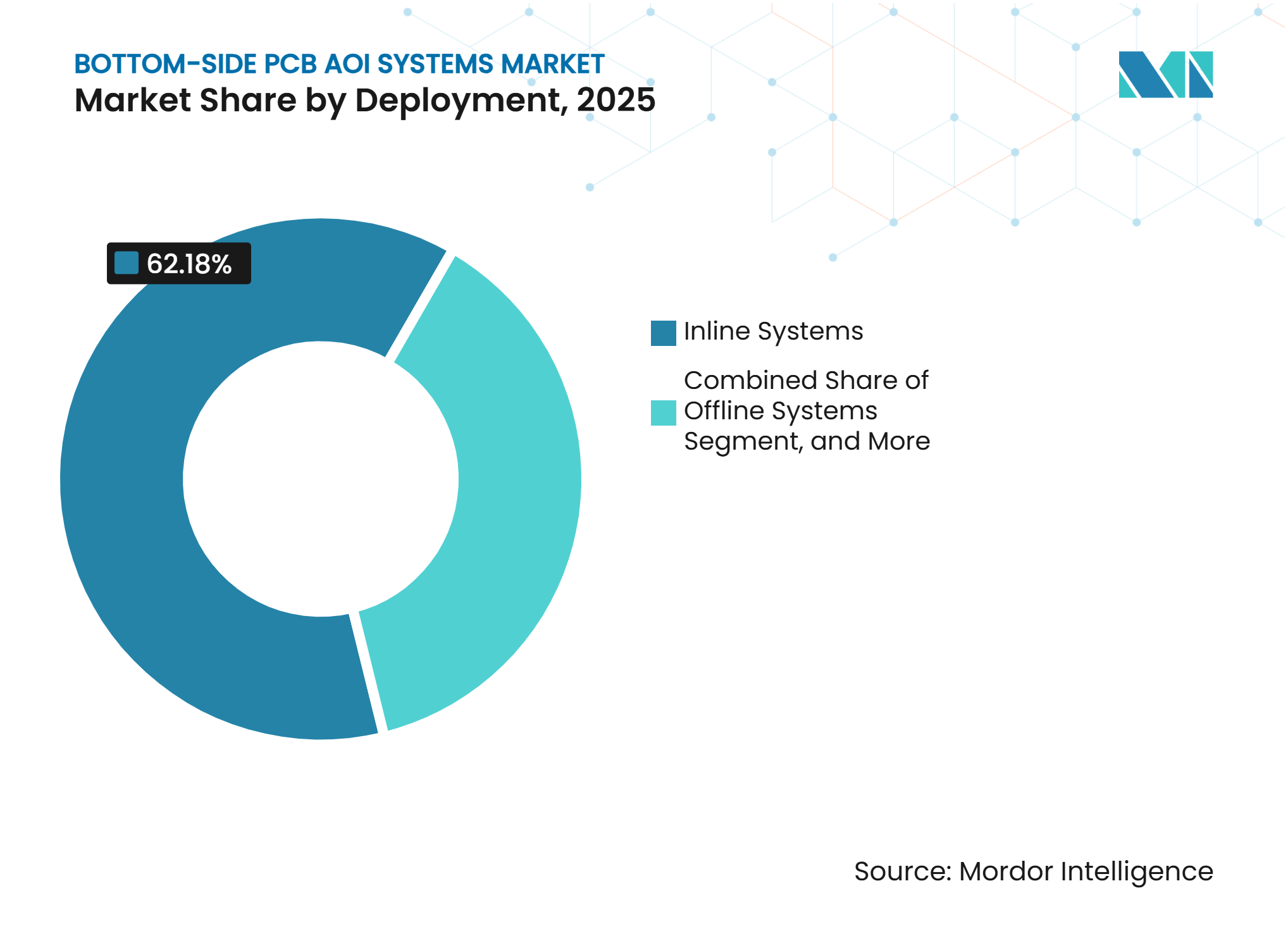
Inspection-Island Systems Support Flexible ManufacturingInline systems accounted for 62.18% of the deployment share in 2025. Their position reflects the production needs of high-volume PCB lines, where a separate inspection step can interrupt board flow. An inline system can identify recurring insufficient-solder patterns and alert operators before a batch proceeds. It can also provide data for selective soldering recipe adjustments. This configuration remains central to the bottom-side PCB AOI systems market for continuous production environments.
Inspection-island systems are projected to expand at a 9.71% CAGR through 2031. They suit high-mix, low-volume manufacturing and new-product-introduction work, where batch sizes may not support fixed inline tooling for every board. ASYS launched AISPECTURE at PCIM Europe in June 2026 with 3D laser scanning, high-resolution 2D imaging, and customer-specific AI models. Offline systems remain relevant for aerospace, defense, medical imaging, and satellite communications boards that justify manual handling and detailed multi-angle inspection. Users can also apply offline inspection to establish quality baselines before setting inline production parameters. This is useful during new product introduction, when manufacturers need to understand acceptable joint appearance before volume output begins. Some inspection-island systems can be moved between lines as product requirements change. This reduces the historical separation between offline and island deployments. The bottom-side PCB AOI systems market can therefore serve both development work and production support with adaptable platforms.
By End-User Industry:
Automotive Electronics Is Raising Inspection RequirementsElectronics manufacturing held 29.36% share of the market in 2025. The segment is supported by large contract assembly volumes for consumer devices, networking equipment, and industrial controls across Asia-Pacific. Bottom-side inspection is a routine step after wave and selective soldering in these facilities. Consumer electronics and telecommunications customers remain cost-sensitive and continue to rely heavily on 2D inline systems. Smaller passives and tighter component pitches are nonetheless increasing the need for more detailed inspection over time.
Automotive electronics is projected to expand at a 10.68% CAGR through 2031. Electric vehicles and driver-assistance systems add battery-management boards, on-board chargers, DC-DC converters, and radar- or lidar-processing boards. These applications increase PCB content compared with conventional internal-combustion vehicles. Industrial electronics, aerospace and defense, and medical devices also require reliable inspection of dense through-hole arrays and high-current connections. The bottom-side PCB AOI industry serves these users with systems that export board-level records for quality management and regulatory documentation. Industrial control products often include relay boards, variable-frequency drives, motor controllers, and power-conversion modules. These products use dense connector arrays and high-current connections that need reliable solder inspection under vibration and thermal load. Aerospace and defense boards require documented serial-number inspections, while medical devices require evidence of patient-critical assembly inspections. These use cases sustain demand beyond the broader electronics manufacturing segment.
Geography Analysis
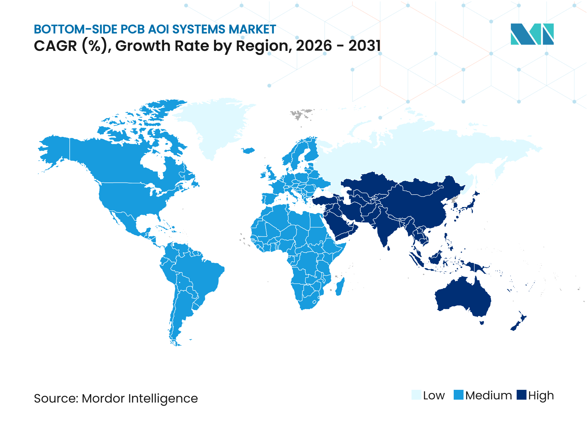
Asia-Pacific held 44.27% share of the regional total in 2025 and is projected to expand at a 10.09% CAGR through 2031. China’s PCB output reached CNY 346.14 billion in 2025 after expanding 17.94% from the prior year. High-density-interconnect boards recorded significant growth, while high-layer-count multilayer boards increased substantially. Japan’s PCB output was projected to grow, supported by AI servers, power electronics, and automotive applications. South Korea and Taiwan contribute advanced-node and automotive-grade production, while Vietnam and Malaysia are receiving capacity shifting from China. India recorded substantial electronics manufacturing output and offers capital subsidies, while Koh Young established a branch in Noida in September.[3]
Europe is the second-largest regional market, with Germany serving as the main automotive inspection center. Automotive electronics, including battery management, inverter control, and driver-assistance boards, are a major source of local demand for 3D AOI. The bottom-side PCB AOI systems market in the region is shaped by quality expectations at automotive Tier 1 and Tier 2 suppliers. Eastern European production centers in Poland, the Czech Republic, and Hungary offer an opportunity to replace older 2D and manual practices as they are upgraded. Vendors must also meet machinery safety and CE marking requirements when selling systems to regulated European facilities.
North America is the third-largest region, supported by aerospace and defense electronics, medical device production, and the expansion of domestic EMS capacity. Facilities established with CHIPS and Science Act incentives are specifying inline 3D AOI at the initial line-design stage. This supports higher average selling prices for the bottom-side PCB AOI systems market. South America is smaller, but it is strengthening its automotive electronics assembly for North American vehicle programs. The Middle East and Africa have demand in the UAE and South Africa, with Saudi Arabia’s Vision 2030 manufacturing zones expected to create further equipment requirements through 2031. The regional opportunity is still in its early stages, so vendors need local service and application support. In South America, automotive programs can increase the use of traceable inspection as supplier standards converge with those in North America. New greenfield lines in North America offer suppliers the opportunity to specify 3D systems from the outset. Across these regions, the bottom-side PCB AOI systems market is shaped by local manufacturing investment and the ability to support regulated production.
Competitive Landscape
Market Concentration
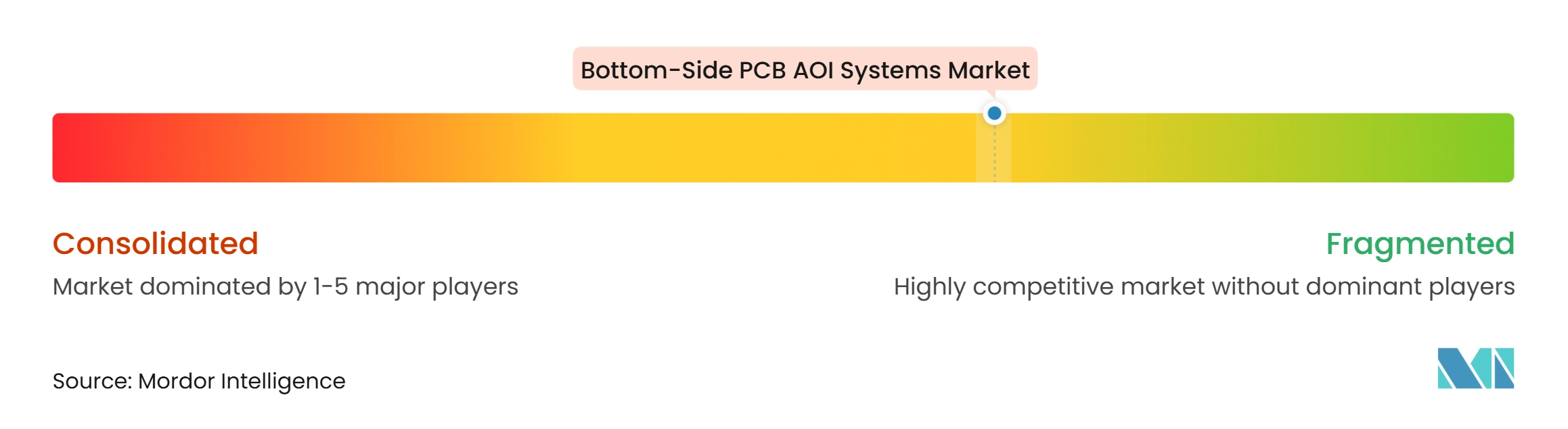
The bottom-side PCB AOI systems market is moderately fragmented. Koh Young Technology and MIRTEC have strong brand positions in True 3D measurement and inspection accuracy, while Taiwanese, European, and Chinese suppliers compete across different price and service positions. A small group offers solder-paste inspection, top-side AOI, and bottom-side AOI as part of a broader portfolio. These companies compete for platform-standardization decisions at large EMS and automotive Tier 1 accounts. Their broader portfolios can simplify equipment selection for customers who want consistent data practices across multiple inspection steps. Specialist suppliers can remain competitive where a buyer needs a lower-cost configuration, local service, or a focused application solution. This creates a two-tier competitive structure rather than a market controlled by one supplier group. The bottom-side PCB AOI systems market remains open to both established portfolio vendors and specialized entrants. A wider group of specialists competes through localized support, pricing, and application-specific customization for smaller assembly operations.
Competition is shifting from rule-based systems to AI-supported inspection and programming. Delvitech stated that its ATON platform processes more than 40 gigabits of inspection data per second through proprietary neural networks to provide 360-degree joint coverage. PARMI’s Xceed BSI uses AI Teaching to create inspection programs in less than 3 minutes without Gerber files. Koh Young introduced the Zenith 2 UHS True 3D AOI system and its Revolution to Success software platform at APEX EXPO 2026. These moves focus on higher-mix production, auto-programming, closed-loop process control, and inspection-data management. Delvitech, PARMI, and Koh Young illustrate a focus on software and data to differentiate similar optical measurement capabilities. The ability to create a program quickly is especially important for contract manufacturers with frequent product changeovers. Closed-loop tools also help customers use AOI results to adjust upstream printing, placement, and soldering processes. This direction gives the bottom-side PCB AOI systems market a stronger link to manufacturing software and process control.
Inspection-island systems for high-mix new-product introduction remain a competitive opening because many established platforms were designed for high-volume inline performance. Flexible and rigid-flex boards for wearable medical devices and aerospace sensor modules also require configurable fixturing and non-contact height sensing. Tier 2 and Tier 3 automotive suppliers in South and Southeast Asia form another opportunity as quality requirements move further down the supply chain. Chinese vendors, including JUTZE Intelligence Technology, Sinic-Tek Vision Technology, and Shenzhen JT Automation Equipment, are competing in this tier. ## Recent Industry Developments
Bottom-Side PCB AOI Systems Industry Leaders
-
Viscom SE
-
SAKI Corporation
-
PARMI Co., Ltd.
-
PEMTRON Corporation
-
ViTrox Corporation Berhad
- *Disclaimer: Major Players sorted in no particular order
Bottom-Side PCB AOI Systems Market Companies Covered in this Report
- Koh Young Technology Inc.
- Viscom SE
- SAKI Corporation
- PARMI Co., Ltd.
- PEMTRON Corporation
- ViTrox Corporation Berhad
- Test Research, Inc.
- MIRTEC CO., LTD.
- GÖPEL electronic GmbH
- Delvitech SA
- JUTZE Intelligence Technology Co., Ltd.
- ALeader Vision Technology Co., Ltd.
- Machvision Inc.
- Mek Marantz Electronics Ltd.
- Machine Vision Products, Inc.
- YESTECH, Inc.
- Sinic-Tek Vision Technology Co., Ltd.
- ZhenHuaXing Technology Co., Ltd.
- Shenzhen JT Automation Equipment Co., Ltd.
- TechValley Co., Ltd.
- ASC International, Inc.
- Utechzone Co., Ltd.
- FAVITE, Inc.
- CIMS Co., Ltd.
- Magic-ray Technology Co., Ltd.
- Pure-Play Manufacturer Qualification and Exclusion Criteria
Recent Industry Developments in Bottom-Side PCB AOI Systems Market
- September 2026: Koh Young Technology announced the establishment of a new branch office in Noida, Uttar Pradesh, India, to strengthen technical applications and business development support for the country’s expanding electronics manufacturing sector, marking a formal regional infrastructure commitment aligned with India’s growing PCB assembly capacity
- September 2026: Koh Young showcased its Meister series 3D semiconductor inspection platforms, including the ZenStar wafer-level packaging inspection system, at SEMICON Taiwan 2026 from September 2 to 4, signaling a strategic expansion from PCB-level AOI into advanced semiconductor packaging inspection.
- June 2026: ASYS Group launched the AISPECTURE AOI system at PCIM Europe 2026, described as the world’s first truly unsupervised inspection platform for power electronics manufacturing. It combines 3D laser scanning, high-resolution 2D imaging, and customer-specific AI models, with no training images or manual parameterization required, directly addressing the high-mix, small-batch production challenge.
- March 2026: Koh Young unveiled multiple new machine platforms at APEX EXPO 2026, including the Zenith 2 UHS True 3D AOI system and the Revolution to Success unified software platform, targeting higher-mix production with AI-driven auto-programming, closed-loop process control, and improved inspection-data management across connected lines.
Global Bottom-Side PCB AOI Systems Market Report Scope
A Bottom-Side PCB AOI Systems market comprises the revenues generated from the sale, installation, software, and associated support of automated optical inspection equipment specifically designed to inspect the underside of assembled printed circuit boards (PCBAs). These systems use machine-vision cameras, lighting, image-processing software, and, where applicable, three-dimensional measurement to identify defects in components, solder joints, pins, pads, markings, and assembly quality without requiring manual visual inspection. AOI is a non-contact inspection method used to detect issues such as missing or misplaced components, solder bridges, insufficient solder, lifted leads, polarity errors, non-wetting, and through-hole soldering defects
The Bottom-Side PCB AOI Systems Market Report is Segmented by Product Type (2D Bottom-Side AOI Systems, 3D Bottom-Side AOI Systems, Hybrid 2D and 3D Bottom-Side AOI Systems), Inspection Stage (Pre-Soldering, Post-Reflow, Post-Wave Soldering, Post-Selective Soldering, Final Assembly and Rework Verification), Deployment (Inline Systems, Offline Systems, and Inspection-Island Systems), End-User Industry (Electronics Manufacturing, Automotive Electronics, Industrial Electronics, Aerospace and Defense Electronics, Consumer Electronics, Medical Devices, Telecommunications and Networking, Other End-User Industries\), and Geography (North America, South America, Europe, Asia-Pacific, and Middle East and Africa). The Market Forecasts are Provided in Terms of Value (USD).
Segmentation Overview
| 2D Bottom-Side AOI Systems |
| 3D Bottom-Side AOI Systems |
| Hybrid 2D and 3D Bottom-Side AOI Systems |
| Pre-Soldering Inspection |
| Post-Reflow Inspection |
| Post-Wave Soldering Inspection |
| Post-Selective Soldering Inspection |
| Final Assembly and Rework Verification |
| Inline Systems |
| Offline Systems |
| Inspection-Island Systems |
| Electronics Manufacturing |
| Automotive Electronics |
| Industrial Electronics |
| Aerospace and Defense Electronics |
| Consumer Electronics |
| Medical Devices |
| Telecommunications and Networking |
| Other End-User Industry |
| North America | United States | |
| Canada | ||
| Mexico | ||
| South America | Brazil | |
| Argentina | ||
| Rest of South America | ||
| Europe | Germany | |
| United Kingdom | ||
| France | ||
| Italy | ||
| Spain | ||
| Rest of Europe | ||
| Asia-Pacific | China | |
| Japan | ||
| India | ||
| South Korea | ||
| ASEAN | ||
| Rest of Asia-Pacific | ||
| Middle East and Africa | Middle East | Saudi Arabia |
| United Arab Emirates | ||
| Turkey | ||
| Rest of the Middle East | ||
| Africa | South Africa | |
| Nigeria | ||
| Rest of Africa | ||
| By Product Type | 2D Bottom-Side AOI Systems | ||
| 3D Bottom-Side AOI Systems | |||
| Hybrid 2D and 3D Bottom-Side AOI Systems | |||
| By Inspection Stage | Pre-Soldering Inspection | ||
| Post-Reflow Inspection | |||
| Post-Wave Soldering Inspection | |||
| Post-Selective Soldering Inspection | |||
| Final Assembly and Rework Verification | |||
| By Deployment | Inline Systems | ||
| Offline Systems | |||
| Inspection-Island Systems | |||
| By End-User Industry | Electronics Manufacturing | ||
| Automotive Electronics | |||
| Industrial Electronics | |||
| Aerospace and Defense Electronics | |||
| Consumer Electronics | |||
| Medical Devices | |||
| Telecommunications and Networking | |||
| Other End-User Industry | |||
| By Geography | North America | United States | |
| Canada | |||
| Mexico | |||
| South America | Brazil | ||
| Argentina | |||
| Rest of South America | |||
| Europe | Germany | ||
| United Kingdom | |||
| France | |||
| Italy | |||
| Spain | |||
| Rest of Europe | |||
| Asia-Pacific | China | ||
| Japan | |||
| India | |||
| South Korea | |||
| ASEAN | |||
| Rest of Asia-Pacific | |||
| Middle East and Africa | Middle East | Saudi Arabia | |
| United Arab Emirates | |||
| Turkey | |||
| Rest of the Middle East | |||
| Africa | South Africa | ||
| Nigeria | |||
| Rest of Africa | |||
Key Questions Answered in the Report
What is the bottom-side PCB AOI systems market size?
The bottom-side PCB AOI systems market size is estimated at USD 454.82 million in 2026 and is forecast to reach USD 704.01 million by 2031, at a 9.13% CAGR.
Why is 3D bottom-side inspection gaining adoption?
3D systems provide height and solder-volume information that supports inspection of high-reliability through-hole joints in automotive, aerospace, and industrial electronics.
Which product type led demand in 2025?
2D bottom-side AOI systems led with a 55.27% share in 2025 because they offer lower cost and fast setup for high-volume assembly lines.
Which inspection stage is expanding fastest?
Post-selective soldering inspection is projected to expand at a 10.12% CAGR through 2031 as manufacturers use selective soldering to protect heat-sensitive components.
Which region leads demand for bottom-side PCB AOI equipment?
Asia-Pacific led with a 44.27% share in 2025 and is projected to expand at a 10.09% CAGR through 2031, supported by its extensive PCB assembly base.
What limits adoption of bottom-side AOI systems?
High equipment and integration costs, along with programming demands in high-mix production, can delay deployment at smaller assembly operations.