Market Trends of 3D TSV Devices Industry
This section covers the major market trends shaping the 3D TSV Devices Market according to our research experts:
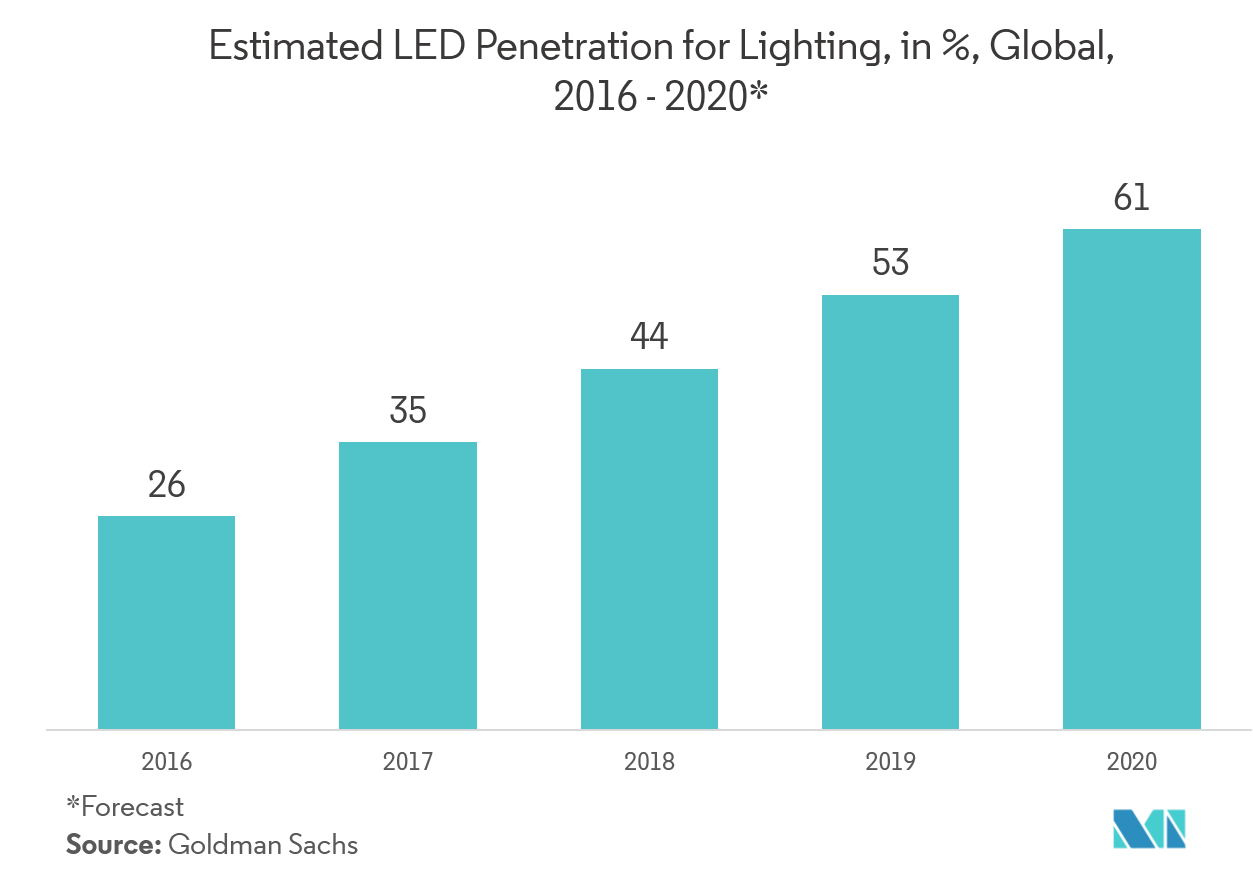
LED Packaging Will Have a Significant Market Share
- The increasing use of light-emitting diodes (LED) in products has promoted the development of higher power, greater density, and lower-cost devices. The use of three-dimensional (3D) packaging through-silicon via (TSV) technology allows a high density of vertical interconnects, unlike 2D packaging.
- TSV integrated circuit reduced connection lengths, and thus, smaller parasitic capacitance, inductance, and resistance are required where a combination of monolithic and multifunctional integration is done efficiently, which provides high-speed low-power interconnects.
- The embedded design with thin silicon membranes at the bottom optimizes the thermal contact and therefore minimizes the thermal resistance. Through silicon via (TSV) provides the electrical contact to the surface-mounted devices and mirrored sidewalls increase the package reflectivity and improve the light efficiency.
- The SUSS AltaSpray technology is capable of coating integration of 90° corners, KOH (Potassium Hydroxide) etched cavities, Through Silicon Via (TSV) ranging from a few microns to 600μm or more. The ability to produce conformal resist coatings on severe topography, such as TSV, makes them the ideal choice for wafer-level packaging in LED, which increases the market growth.
Understand The Key Trends Shaping This Market
Download Sample
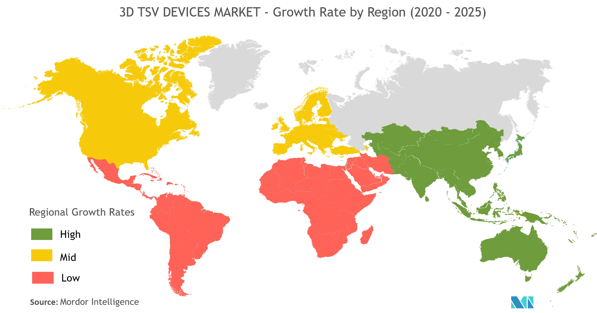
Asia-Pacific to Witness the Fastest Growth Rate Over the Forecast Period
- Asia-Pacific is the fastest-growing market as countries in the region, such as China, Japan, South Korea, Indonesia, Singapore, and Australia, have recorded high levels of manufacturing in the consumer electronics, automotive, and transportation sectors, which a key source of demand for 3D TSV market.
- Asia-Pacific is also one of the most active manufacturing hubs in the world. The rising popularity of smartphones and demand for new memory technologies have increased the growth of computationally intensive consumer electronics, thereby, creating a wide range of opportunities in this region. As silicon wafers are widely used to manufacture smartphones, the introduction of 5G technology is expected to boost the sales of 5G smartphones, which may grow the market in the telecommunication sector.
- In April 2019, in Korea, a collective laser‐assisted bonding process for 3D TSV integration with NCP( nonconductive paste) is made, where several TSV dies can be stacked simultaneously to improve the productivity while maintaining the reliability of the solder joints through Laser‐assisted bonding (LAB) advanced technology. These solder joints may increase the growth in consumer and commercial segments, which may increase the growth of the market.
Get Analysis on Important Geographic Markets
Download Sample
