Market Trends of 3D IC Packaging Industry
This section covers the major market trends shaping the 3D IC Packaging Market according to our research experts:
IT & Telecommunication is Expected to Witness Significant Growth
- 3D IC Packaging is an essential part of semiconductor manufacturing and design. It directly affects performance, power, and cost on a macro level and the basic functionality of all chips on a micro level.
- The increasing investment in 5G infrastructure and the growing number of data center servers coupled with IoT connections and networking devices are the factors propelling the growth of 3D IC packaging in the IT and telecommunication sector. For instance, mobile operators in Korea such as KT, LG Uplus, and SK Telecom agreed to invest a total of KRW 25.7 trillion through 2022 to support 5G infrastructure across the country. The additional investment is focused on enhancing the 5G quality in Seoul and six other cities.
- The expansion of data centers provides a growth opportunity for the vendors in the 3D IC packaging studied. According to Cisco Systems, the amount of big data in data center storage global is anticipated to reach 403 exabytes in 2021, with a significant share in the US. Hyperscale data centers reached 700 in 2021, compared to 259 in 2015.
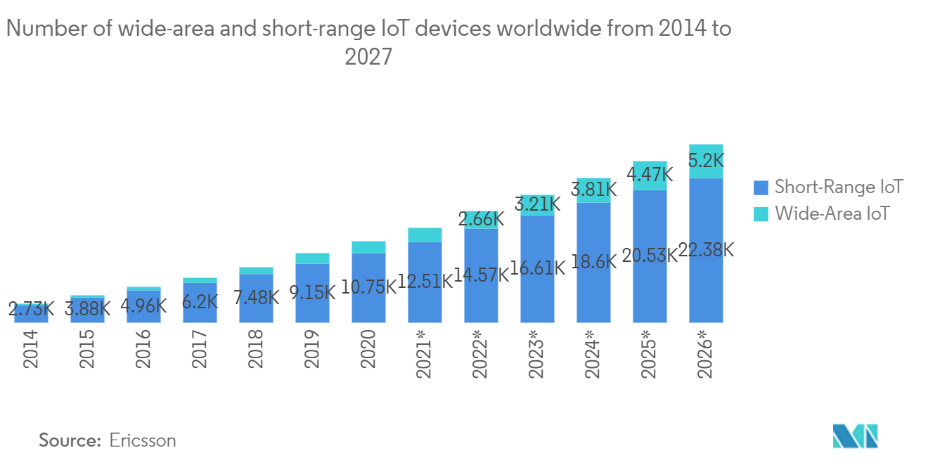
- Moreover, the growing IoT market and surging demand for wireless technologies, wherein reduced footprint and enhanced efficiency are critical, are expected to develop the market for 3D IC packaging. According to Ericson, wide-area IoT devices will reach 5.2 billion by 2027 from 2.1 billion in 2021.
Understand The Key Trends Shaping This Market
Download Sample
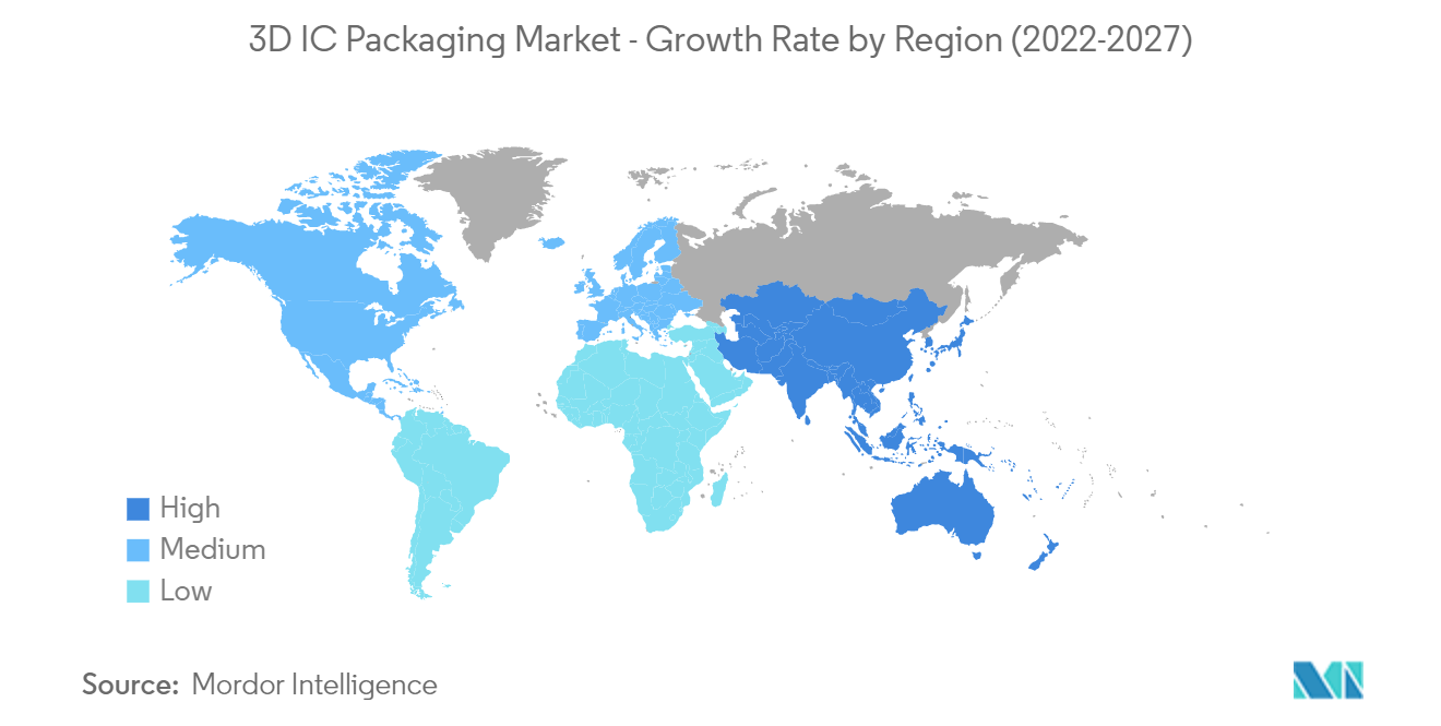
Asia-Pacific is Expected to Witness Significant Growth Rate
- Asia Pacific is home to some of the biggest semiconductor chip manufacturers and companies like TSMC, SMIC, UMC, and South Korea's Samsung. Taiwan's leading chip foundry is teaming up with Japanese suppliers in the race to lead the crucial 3-nanometer chip market. For instance, in February 2021, TSMC announced that the company plans to establish an R&D center in Japan's science city of Tsukuba to develop 3D IC packaging materials in cooperation with its Japanese suppliers.
- Also, in May 2021, Japan's Ministry of Economy, Trade, and Industry and its subsidiary, the National Institute of Advanced Industrial Science and Technology, announced that approximately 20 Japanese companies would work with TSMC Japan's 3D IC R&D Center.
- The Asia Pacific region also holds a significant share in the 3D IC packaging market due to a considerable number of semiconductor manufacturing operations happening in the region, along with the presence of major market players such as Samsung Electronics Co., Ltd., Toshiba Corp, ASE Group, and United Microelectronics Corp. among others.
- The Asia Pacific region is known for its robust Automotive manufacturing capabilities. Moreover, the growing commercialization of 5G technology in the automotive industry will provide a new revenue stream for the vendors operating in the studied market. The advent of 5G NR-based C-V2X is anticipated to offer unique capabilities for the autonomous vehicle. Thus, it can propel the need for higher levels of autonomy and predictability and other ADAS sensor technologies in the vehicle.
- Additionally, market players in the region are forcing on Next-gen chip technology, which could unlock new potential with 3D packaging tools. For instance, Japanese tool-making company Disco focuses on 3D chip packaging by stacking integrated circuits on silicon wafers of near-transparent thinness. As Moore's Law nears its physical limits, chipmakers seek new designs and materials to get better performance out of next-generation hardware. Such trends are expected to propel growth in the region.
- In the current scenario of smart devices and the connected world, customers demand next-generation devices that are more compact, multi-functional, offer better performance, and consume less power. This has propelled the demand for cost-efficient and high-performance IC. For instance, STAR's Institute of Microelectronics has partnered with leading semiconductor companies to develop cost-effective 3D wafer-level integrated circuit packaging solutions. The company has launched chip-on-wafer consortium II and the cost-effective Interposer consortium to advance chip packaging solutions for high-volume manufacturing. The industry-focused consortium will address key challenges in wafer-level packaging to low overall manufacturing costs to accelerate time-to-market for next-generation electronics devices.
Get Analysis on Important Geographic Markets
Download Sample
