
UV Imaging Market Size and Share
Market Overview
| Study Period | 2020 - 2031 |
|---|---|
| Market Size (2026) | USD 594.86 Million |
| Market Size (2031) | USD 942.29 Million |
| Growth Rate (2026 - 2031) | 9.64 % |
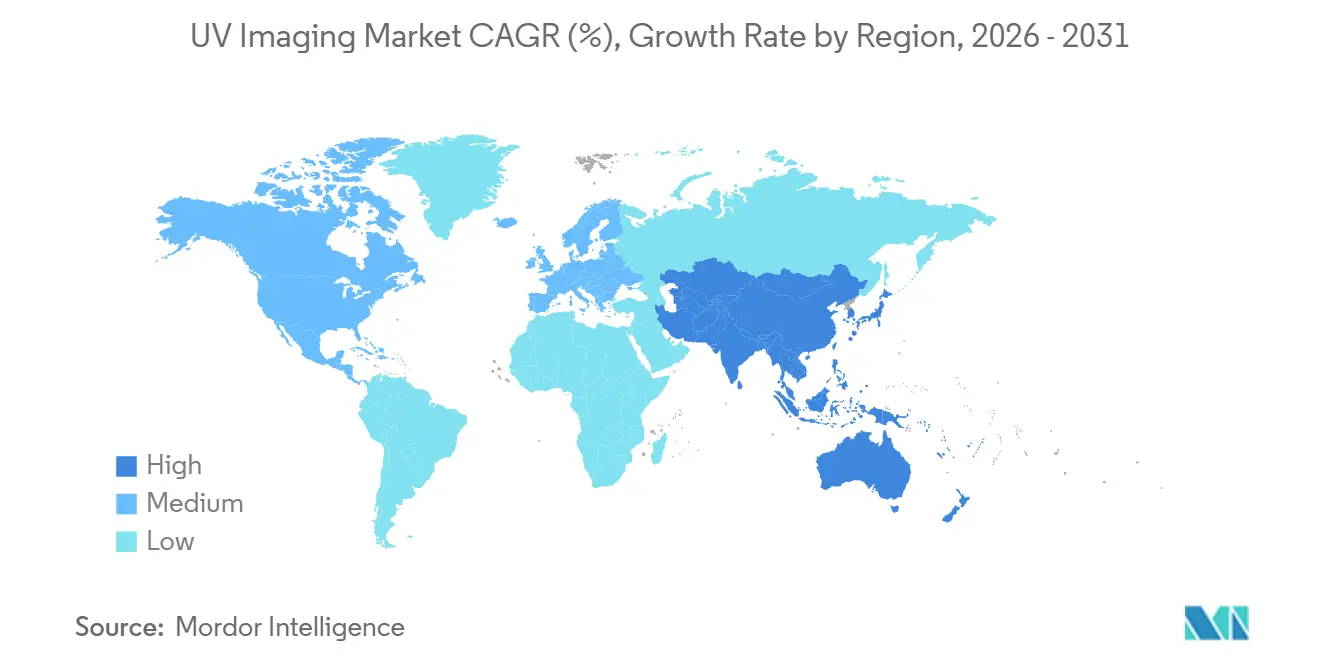
| Fastest Growing Market | Asia-Pacific |
| Largest Market | North America |
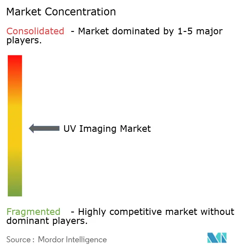
| Market Concentration | Medium |
Major Players *Disclaimer: Major Players sorted in no particular order Image © Mordor Intelligence. Reuse requires attribution under CC BY 4.0. | |
UV Imaging Market Analysis by Mordor Intelligence
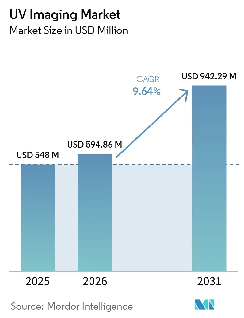
The UV imaging market size was valued at USD 548 million in 2025 and is estimated to expand from USD 594.86 million in 2026 to reach USD 942.29 million by 2031, at a CAGR of 9.64% during the forecast period 2026-2031. Demand is broadening across power infrastructure, semiconductor fabrication, pharmaceutical quality control, and forensic inspection. This wider application base reduces dependence on a single use case. Networked monitoring systems are replacing standalone inspection tools in many deployments. These systems can add software revenue and reduce reliance on one-time hardware sales. Data center construction also supports demand for semiconductor inspection, extending replacement cycles for UV imaging equipment.
Key Report Takeaways
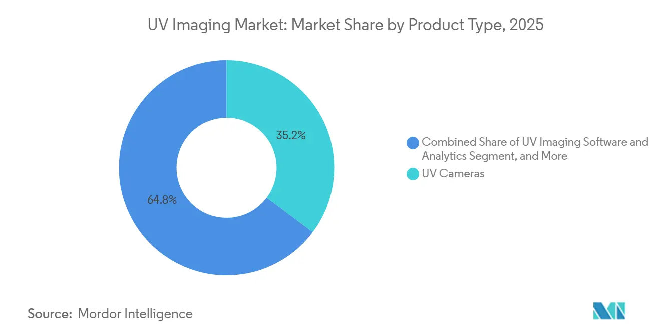
- By product type, UV cameras held 35.15% share of the UV imaging market in 2025, while UV integrated systems are projected to expand at a 12.52% CAGR through 2031.
- By spectrum range, near UV [315-400 nm] held 44.27% share of the UV imaging market in 2025, while far / vacuum UV [100-280 nm] is projected to expand at an 11.79% CAGR through 2031.
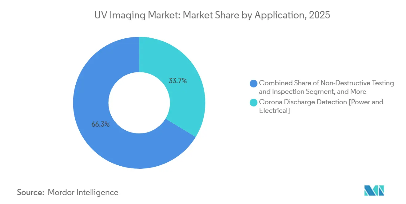
- By application, corona discharge detection held 33.67% share of the UV imaging market in 2025, while fluorescence analysis is projected to expand at a 12.05% CAGR through 2031.
- By end-user industry, power transmission and distribution held 34.21% share of the UV imaging market in 2025, while healthcare and life sciences are projected to expand at an 11.92% CAGR through 2031.
- By geography, North America held 31.45% share of the UV imaging market in 2025, while Asia-Pacific is projected to expand at a 12.02% CAGR through 2031.
Note: Market size and forecast figures in this report are generated using Mordor Intelligence’s proprietary estimation framework, updated with the latest available data and insights as of January 2026.
Market Trends and Insights
Drivers Impact Analysis of UV Imaging Market*
| Driver | (~) % Impact on CAGR Forecast | Geographic Relevance | Impact Timeline |
|---|---|---|---|
| Semiconductor and Advanced Packaging Inspection Intensity | +2.1% | East Asia, North America, Europe | Short term (≤ 2 years) |
| Expansion of Automated Zero-Defect Manufacturing | +1.9% | Global, with strength in Germany, Japan, South Korea, and China | Medium term (2-4 years) |
| Live High-Voltage Asset Condition Monitoring | +1.5% | North America, Europe, South and Southeast Asia | Short term (≤ 2 years) |
| UV LED Cost and Efficiency Improvements | +1.2% | Global | Medium term (2-4 years) |
| AI-Assisted Defect Classification and Remote Inspection | +1.0% | Global, with early adoption in North America and East Asia | Medium term (2-4 years) |
| UV Fluorescence and Anti-Counterfeit Inspection Expansion | +0.7% | Europe, North America, Asia-Pacific | Long term (≥ 4 years) |
| Source: Mordor Intelligence | |||
Semiconductor And Advanced Packaging Inspection Intensity
Advanced packaging uses 3D integration, chiplets, and heterogeneous stacking, thereby increasing defect sensitivity requirements. The UV imaging market benefits from shorter wavelengths, which reveal nanoscale surface features. UV systems operating from 200 nm to 400 nm can detect particles and pattern-edge irregularities that standard optics can miss. Sony's IMX487 global-shutter UV sensor operates across this range at up to 193 frames per second in 10-bit mode. This performance supports full-surface inspection at production-line speeds. The UV imaging market can therefore benefit from increasingly demanding quality requirements in advanced semiconductor production.[1]
Expansion Of Automated Zero-Defect Manufacturing
Manufacturers are moving from statistical sampling toward 100% in-line optical inspection. UV imaging is useful where surface integrity requirements exceed those of visible light. Research presented at CVPR 2026 found that spectral-domain architectures outperformed conventional vision baselines by at least 19.7% in open-set defect localization. Such approaches can help lines identify failure modes absent from the training data. Real-time tablet measurement systems have also reached throughputs of up to 360,000 tablets per hour with relative prediction errors below 5%. These operating results support the deployment of UV imaging in situations where destructive sampling is costly.
Live High-Voltage Asset Condition Monitoring
Aging transmission and distribution networks are increasing use of live-voltage corona inspection. The American Society of Civil Engineers assigned the United States energy grid a D+ in its 2025 Infrastructure Report Card. Solar-blind cameras detect UV-C emissions from air ionization around high-voltage equipment. They can find developing faults before thermal anomalies are visible. In April 2026, moviTHERM and Ofil Systems integrated UV corona detection into the iTL thermal monitoring platform. The common cloud interface supports simultaneous thermal and UV alerting for fixed-point substation monitoring.
UV LED Cost And Efficiency Improvements
Improved aluminum gallium nitride (AlGaN) emitters are making compact mercury-free illumination more practical. Nichia began mass production of its 280 nm NCSU434D deep UV LED in December 2024. The product delivered 7.4% wall-plug efficiency at 350 mA, compared with 3.1% in the 2021 baseline. Stanley Electric reported 7.5% wall-plug efficiency for a 265 nm UV-C LED in March 2026. It also reported an L70 lifetime of 25,000 hours, with mass production planned for October 2026. These advances strengthen the case for the UV imaging market by reducing illumination costs in both integrated lines and portable field systems.
Restraints Impact Analysis of UV Imaging Market*
| Restraint | (~) % Impact on CAGR Forecast | Geographic Relevance | Impact Timeline |
|---|---|---|---|
| UV-Compatible Optics and Sensor Packaging Cost | -1.5% | Global, strongest in price-sensitive South and Southeast Asian and African markets | Short term (≤ 2 years) |
| UV Sensor Degradation and Calibration Burden | -1.1% | Global, especially outdoor continuous-monitoring deployments | Medium term (2-4 years) |
| Specialized Component Supply Concentration | -0.8% | Global, with greater exposure under trade restrictions | Long term (≥ 4 years) |
| Regulatory Validation Complexity for Medical and Environmental Uses | -0.5% | Europe and North America, with rising relevance in Asia-Pacific | Long term (≥ 4 years) |
| Source: Mordor Intelligence | |||
UV-Compatible Optics And Sensor Packaging Cost
Fused silica and calcium fluoride, CaF₂, optics cost more than borosilicate glass for transmission below 350 nm. Deep UV lenses also need precise polishing and controlled production facilities. UV-enhanced silicon CMOS sensors require anti-reflection coatings and UV-transparent windows. They may also require removal of the native SiO₂ passivation layer. JENOPTIK lens assemblies for 193 nm and 266 nm inspection require mounting precision below 10 nanometers. These requirements restrict the supplier base and keep systems beyond the budget of many general inspection applications.[2]
UV Sensor Degradation And Calibration Burden
High-energy UV photons can reduce photocathode efficiency and CMOS pixel responsivity over time. They can also degrade anti-reflection coatings, especially below 300 nm. A 2025 review found that many commercial UV-C LEDs had L70 lifetimes of only a few thousand hours. This differs from leading controlled-condition results such as Stanley Electric's 25,000-hour result at 265 nm. Outdoor substations and sterilization validation lines may therefore require periodic recertification and source replacement. The added maintenance recordkeeping can affect total ownership costs and constrain UV imaging market adoption where maintenance budgets are limited.
*Our forecasts treat driver/restraint impacts as directional, not additive. The impact forecasts reflect baseline growth, mix effects, and variable interactions.
UV Imaging Market Segment Analysis
By Product Type, Integrated Systems Support Automated Inspection
UV cameras held 35.15% of the UV imaging market share in 2025, and their established uses include corona discharge inspection, non-destructive testing, and laboratory fluorescence analysis. Solar-blind cameras are widely used for corona work because they limit solar background interference; their photocathodes are sensitive mainly to the 240-280 nm UV-C band. This spectral selectivity supports daytime inspection of live high-voltage equipment. Broadband cameras covering 200-400 nm are used in semiconductor and life sciences environments. They generally need controlled illumination and filtering to preserve contrast. These conditions make them less suitable for many outdoor field uses.
Integrated systems are projected to record the fastest product-category CAGR of 12.52% through 2031, and the UV imaging market size for these systems is supported by automation programs that combine UV, visible, and infrared modules, unified acquisition frameworks place priority on throughput and data management, Sony designed the IMX487 for inline applications at up to 193 frames per second, the sensor supports imaging across 200-400 nm within high-throughput equipment. Software and analytics are also becoming important within this product group. AI-based classification and severity scoring can reduce reliance on operator interpretation. IEC 62443 is increasingly relevant when inspection platforms connect to plant networks and cloud services.

By Spectrum Range, Far/Vacuum UV Extends Beyond Research Labs
Near UV accounted for 44.27% of the UV imaging market share in 2025, reflecting compatibility with UV-A LEDs, glass optics, and standard silicon sensors. This combination makes near-UV the more accessible option for many users; common uses include forensic examination, fluorescence material analysis, and quality control. Fluorescent penetrant testing also supports demand for 365 nm UV-A illumination. ASTM E165 identifies this wavelength for relevant testing procedures. Mid UV systems operate from 280 nm to 315 nm. They support protein and nucleic acid analysis, as well as selected atmospheric monitoring tasks.
Far/Vacuum UV from 100 nm to 280 nm is projected to expand at an 11.79% CAGR through 2031, and demand comes from 193 nm and 266 nm lithography inspection, germicidal validation, and vacuum UV spectroscopy, the UV imaging market size for this range reflects increasingly strict semiconductor inspection requirements, JENOPTIK offers objective lenses designed for 193 nm and 266 nm inspection, these systems use fused silica, CaF₂, and MgF₂ optics with specialized sensors. Their cost premium persists for near-UV configurations. IEC 62471 and national exposure requirements also shape UV-C system design. Compliance creates both design constraints and a means of product differentiation.
By Application, Corona Detection Leads While Pharma Fluorescence Advances
Corona discharge detection accounted for 33.67% of the UV imaging market share in 2025. Solar-blind cameras can image corona discharge in daylight without masking or filtering; this capability aligns directly with high-voltage asset monitoring needs. IEC 60270:2000 provides a partial discharge measurement framework for utilities. It supports using UV photon counts for severity classification. Non-destructive testing is another major application cluster. Aerospace, automotive, oil and gas, and precision manufacturers use UV-A penetrant and photoluminescence methods. ASTM E165, ASTM E709, and ISO 3452 support inspection protocols in these sectors.
Fluorescence analysis in the pharmaceutical and life sciences is projected to expand at a 12.05% CAGR through 2031 and supports in-line content uniformity measurement as a process analytical technology application. Real-time UV imaging has inspected more than 300,000 tablets per hour, with prediction errors below 5%. Research has also shown that UV imaging can distinguish tablets produced by batch and continuous blending methods. The reported root-mean-square error of prediction was 0.381 w/w%. Deep-UV fluorescence lifetime imaging at 265 nm has also differentiated cancer-margin tissue from normal tissue. This clinical use would need future validation before wider surgical adoption.
By End-User Industry, Power Utilities Lead While Life Sciences Gain Ground
Power transmission and distribution held 34.21% of the UV imaging market share in 2025, and utilities use UV corona inspection to manage aging high-voltage equipment. Capital programs in North America, Europe, and South and Southeast Asia support this work. Ofil Systems' Gridnostic platform applies AI-based severity scoring to UV corona images and supports a move from periodic manual inspection toward continuous monitoring. That transition adds software and data-service opportunities beyond camera hardware. Oil and gas, aerospace and defense, and industrial manufacturing remain established end-user groups. Their inspection protocols support steady rather than rapid demand.[3]
Healthcare and life sciences are projected to expand at an 11.92% CAGR through 2031, and pharmaceutical quality control and real-time biofilm detection support this outlook. Laser-induced UV fluorescence can detect viable airborne microorganisms in real time. A 2025 validation study examined the use of biofluorescent particle counting in aseptic pharmaceutical filling zones; this approach could support continuous environmental monitoring. Automotive users apply UV inspection for fluorescent magnetic particle and penetrant testing. ASTM E1444/E1444M guides the testing of safety-critical powertrain and chassis components. FDA 21 CFR Part 11 also favors validated platforms with electronic records and audit trails.
Geography Analysis
North America UV Imaging Market
North America held 31.45% of the UV imaging market share in 2025, and aging electricity infrastructure supports demand for corona inspection across the region. The United States also has major semiconductor fabrication investments, and defense procurement adds demand for solar-blind and intensified UV systems. The United States grid received a D+ in the 2025 Infrastructure Report Card. This maintenance gap supports treating diagnostics as grid-reliability investments. Semiconductor capacity programs in Arizona, Ohio, and Texas support high-speed wafer and packaging inspection. Canada and Mexico add demand from industrial manufacturing and oil and gas inspection.
APAC UV Imaging Market
Asia-Pacific is projected to expand at a 12.02% CAGR through 2031, with China, India, Japan, and South Korea driving demand for grid upgrades and semiconductor manufacturing. Pharmaceutical compliance requirements add another source of regional demand. Japan has important component suppliers in Hamamatsu Photonics K.K and Sony Semiconductor Solutions Corporation. Hamamatsu supplies UVTRON flame and discharge sensors, as well as compact Si APD products. Sony supplies the IMX487 UV image sensor for global equipment suppliers. This manufacturing base supports the UV imaging market across core sensing technologies. Asia-Pacific utilities also combine UV inspection with drone-based and AI-assisted sensing platforms.[4]
EMEA and South America UV Imaging Market
Europe held a meaningful position in 2025 through German semiconductor optics and precision photonics manufacturing, while JENOPTIK inaugurated a EUR 100 million (USD 109 million) micro-optics facility in Dresden in May 2025. The company also announced a planned low-double-digit-million-EUR expansion in Jena. The United Kingdom uses UV imaging in forensic work under SWGDE guidance, France remains important in UV-intensified camera technology through Exosens, and South America has earlier-stage demand in oil and gas, agricultural inspection, and authentication. The Middle East and Africa show growing interest in utility transmission reliability and industrial testing. EU Directive 2006/25/EC sets occupational exposure limits that affect European system design.
Competitive Landscape
The UV imaging market has moderate concentration, with vertically integrated photonics groups holding positions in high-sensitivity and defense-rated applications, while application specialists and scientific camera makers compete in narrower segments. Exosens operates UV technology through its Photonis subsidiary; its i2Nocturn series provides single-photon sensitivity across the 190-300 nm UV-C range, JENOPTIK serves the value chain through deep-UV lenses for 193 nm and 266 nm inspection, Ofil Ltd. and UViRCO Technologies Ltd. compete in corona detection with solar-blind platforms. Their competition centers on sensitivity, ergonomics, and analytics integration.
Competition is shifting from individual camera specifications toward integrated capabilities, and Ofil's Gridnostic platform converts UV corona imagery into asset-severity scores inside a grid management interface, this type of software can add switching costs for hardware-only suppliers, Exosens closed its Emberion acquisition in April 2026, adding quantum-dot infrared sensing technology with 25 patent families, the transaction extended Exosens' sensing portfolio into short-wave infrared applications. JENOPTIK also announced a low-double-digit-million-EUR investment to expand manufacturing in Jena in September 2025. Production was targeted for the second half of 2027, subject to approvals. These moves show how component capacity and multispectral systems are becoming competitive priorities.[5]
Patent activity covers photocathode efficiency, CMOS pixel design, and AI-based UV signal interpretation, while regulatory readiness is also becoming more important in utility and pharmaceutical procurement. IEC 62443 cybersecurity considerations apply to connected industrial inspection platforms; FDA 21 CFR Part 11 requirements apply where systems support electronic records in pharmaceutical quality control; and compact UV-LED designs create opportunities in environmental monitoring and authentication. These areas are especially relevant in price-sensitive locations. South Korean and Chinese suppliers are beginning to target this demand with lower-cost camera configurations. The competitive position of incumbents remains strongest in the UV imaging market, where specialized optics, sensitivity, and validated workflows are essential.
UV Imaging Industry Leaders
-
Hamamatsu Photonics K.K.
-
Teledyne FLIR LLC
-
Oxford Instruments
-
Ofil Ltd.
-
JENOPTIK AG
- *Disclaimer: Major Players sorted in no particular order
UV Imaging Market Companies Covered in this Report
- Hamamatsu Photonics K.K.
- Teledyne FLIR LLC
- Oxford Instruments
- Ofil Ltd.
- JENOPTIK AG
- UViRCO Technologies Ltd.
- Sony Semiconductor Solutions Corporation
- Exosens
- Photonis (Exosens)
- Photek Limited
- Excelitas Technologies Corp.
- Thorlabs, Inc.
- Raptor Photonics Ltd.
- Teledyne Photometrics
- Proxivision GmbH
- Invisible Vision GmbH
- Adimec Advanced Image Systems B.V.
- Xenics NV
- PCO AG
Recent Industry Developments in UV Imaging Market
- April 2026: moviTHERM announced that its iTL intelligent thermal monitoring platform integrated UV corona discharge detection through a technology partnership with Ofil Systems. Both thermal and UV data were routed simultaneously to a common cloud-based analytics engine, with either data stream capable of triggering anomaly alerts. The partnership was demonstrated at the IEEE PES Transmission and Distribution Conference and Exposition 2026 in Chicago, targeting aging North American grid infrastructure where pre-failure corona events are not detectable by thermal sensors alone.
- April 2026: Exosens closed the acquisition of Emberion, a Finland- and United Kingdom-based company that designs and manufactures infrared sensors using patented quantum dot imaging technology. Emberion held 25 patent families worldwide at the time of acquisition and generated EUR 0.7 million (USD 0.76 million) in revenue in fiscal 2025. The acquisition extended Exosens' full-spectrum imaging portfolio into short-wave infrared (SWIR, targeting defense drone imaging and semiconductor inspection applications where SWIR channels complement UV data in multispectral inspection platforms.
- March 2026: Stanley Electric Co., Ltd. announced achieving a wall-plug efficiency of 7.5% for its 265 nm UV-C LED device, representing a threefold improvement over its then-current commercial product, ZEUBE265 (2.3% WPE), and an increase in L70 lifetime from 10,000 to 25,000 hours. Samples were available from March 2026, with mass production planned for October 2026, advancing the economics of UV-C illumination for imaging-system integration in water-disinfection validation, germicidal performance monitoring, and compact far-UV inspection systems.
- May 2025: JENOPTIK AG officially inaugurated its new Dresden micro-optics fabrication facility, its largest single capital investment in recent history at EUR 100 million (USD 109 million), with 2,000 m² of ISO 3 and ISO 5 cleanroom production space dedicated to micro-optical sensors and components for deep-ultraviolet and extreme-ultraviolet semiconductor lithography and inspection. The facility consolidated previously distributed Dresden production activities, employed 100 staff, and was designed to address demand for high-precision UV-range optics.
Global UV Imaging Market Report Scope
The UV imaging market encompasses cameras, integrated systems, software, analytics platforms, and accessories that capture and analyze images in the ultraviolet spectrum. The market includes systems operating in near UV [315-400 nm], mid UV [280-315 nm], and far/vacuum UV [100-280 nm], as well as solar-blind and broadband UV cameras deployed on fixed, portable, and drone-mounted platforms. It encompasses systems supporting various imaging functions, including corona discharge detection, non-destructive testing, flame and arc detection, fluorescence analysis, forensic inspection, and environmental and biological monitoring. The market serves organizations of all sizes across end-user verticals, including power generation and transmission, oil and gas, manufacturing, aerospace and defense, life sciences and healthcare, forensics and law enforcement, and environmental monitoring.
The UV Imaging Market Report is Segmented by Product Type (UV Cameras (Solar Blind UV Cameras, and Broadband UV Cameras), UV Imaging Systems / Integrated Systems, and UV Imaging Software and Analytics), Spectrum Range (Near UV [315-400 nm], Mid UV [280-315 nm], and Far / Vacuum UV [100-280 nm]), Application (Corona Discharge Detection [Power and Electrical], Non-Destructive Testing and Inspection, Flame Detection and Fire Safety, Fluorescence Analysis [Pharmaceutical and Life Sciences], Forensic and Security Inspection, Environmental Monitoring, and Other Applications), End-User Industry (Power Transmission and Distribution, Oil and Gas, Aerospace and Defense, Healthcare and Life Sciences, Automotive, Industrial Manufacturing, and Other End-user Industries), and Geography (North America, South America, Europe, Asia-Pacific, and Middle East and Africa). The Market Forecasts are Provided in Terms of Value (USD).
Segmentation Overview
| UV Cameras | Solar Blind UV Cameras |
| Broadband UV Cameras | |
| UV Imaging Systems / Integrated Systems | |
| UV Imaging Software and Analytics |
| Near UV [315-400 nm] |
| Mid UV [280-315 nm] |
| Far / Vacuum UV [100-280 nm] |
| Corona Discharge Detection [Power and Electrical] |
| Non-Destructive Testing and Inspection |
| Flame Detection and Fire Safety |
| Fluorescence Analysis [Pharmaceutical and Life Sciences] |
| Forensic and Security Inspection |
| Environmental Monitoring |
| Other Applications |
| Power Transmission and Distribution |
| Oil and Gas |
| Aerospace and Defense |
| Healthcare and Life Sciences |
| Automotive |
| Industrial Manufacturing |
| Other End-user Industries |
| North America | United States | |
| Canada | ||
| Mexico | ||
| South America | Brazil | |
| Argentina | ||
| Rest of South America | ||
| Europe | Germany | |
| United Kingdom | ||
| France | ||
| Italy | ||
| Spain | ||
| Rest of Europe | ||
| Asia-Pacific | China | |
| Japan | ||
| India | ||
| South Korea | ||
| Rest of Asia-Pacific | ||
| Middle East and Africa | Middle East | Saudi Arabia |
| United Arab Emirates | ||
| Turkey | ||
| Rest of the Middle East | ||
| Africa | South Africa | |
| Nigeria | ||
| Rest of Africa | ||
| By Product Type | UV Cameras | Solar Blind UV Cameras | |
| Broadband UV Cameras | |||
| UV Imaging Systems / Integrated Systems | |||
| UV Imaging Software and Analytics | |||
| By Spectrum Range | Near UV [315-400 nm] | ||
| Mid UV [280-315 nm] | |||
| Far / Vacuum UV [100-280 nm] | |||
| By Application | Corona Discharge Detection [Power and Electrical] | ||
| Non-Destructive Testing and Inspection | |||
| Flame Detection and Fire Safety | |||
| Fluorescence Analysis [Pharmaceutical and Life Sciences] | |||
| Forensic and Security Inspection | |||
| Environmental Monitoring | |||
| Other Applications | |||
| By End-user Industry | Power Transmission and Distribution | ||
| Oil and Gas | |||
| Aerospace and Defense | |||
| Healthcare and Life Sciences | |||
| Automotive | |||
| Industrial Manufacturing | |||
| Other End-user Industries | |||
| By Geography | North America | United States | |
| Canada | |||
| Mexico | |||
| South America | Brazil | ||
| Argentina | |||
| Rest of South America | |||
| Europe | Germany | ||
| United Kingdom | |||
| France | |||
| Italy | |||
| Spain | |||
| Rest of Europe | |||
| Asia-Pacific | China | ||
| Japan | |||
| India | |||
| South Korea | |||
| Rest of Asia-Pacific | |||
| Middle East and Africa | Middle East | Saudi Arabia | |
| United Arab Emirates | |||
| Turkey | |||
| Rest of the Middle East | |||
| Africa | South Africa | ||
| Nigeria | |||
| Rest of Africa | |||
Key Questions Answered in the Report
What Is the UV Imaging Market Size?
The UV imaging market size was USD 594.86 million in 2026 and is projected to reach USD 942.29 million by 2031 at a 9.64% CAGR.
What Is Driving Demand for UV Imaging Systems?
Semiconductor inspection, automated manufacturing, live grid monitoring, and pharmaceutical quality control are expanding demand. Networked systems also combine cameras with software and recurring diagnostic services.
Which Product Type Led UV Imaging Sales?
UV cameras held the largest product share at 35.15% in 2025. Integrated systems are projected to record the fastest product CAGR at 12.52% through 2031.
Which UV Spectrum Range Is Expanding Fastest?
Far/Vacuum UV is projected to expand at an 11.79% CAGR through 2031. Semiconductor inspection, germicidal validation, and vacuum UV spectroscopy support this outlook.
Which Application Had the Largest Share?
Corona discharge detection held 33.67% of application revenue in 2025. Solar-blind cameras support daylight monitoring of developing high-voltage equipment faults.
Which Region Is Expanding Fastest?
Asia-Pacific is projected to expand at a 12.02% CAGR through 2031. Grid modernization, semiconductor manufacturing, and pharmaceutical compliance requirements support regional demand.