Market Trends of Silicon Epitaxial Wafer Industry
This section covers the major market trends shaping the Silicon Epitaxial Wafer Market according to our research experts:
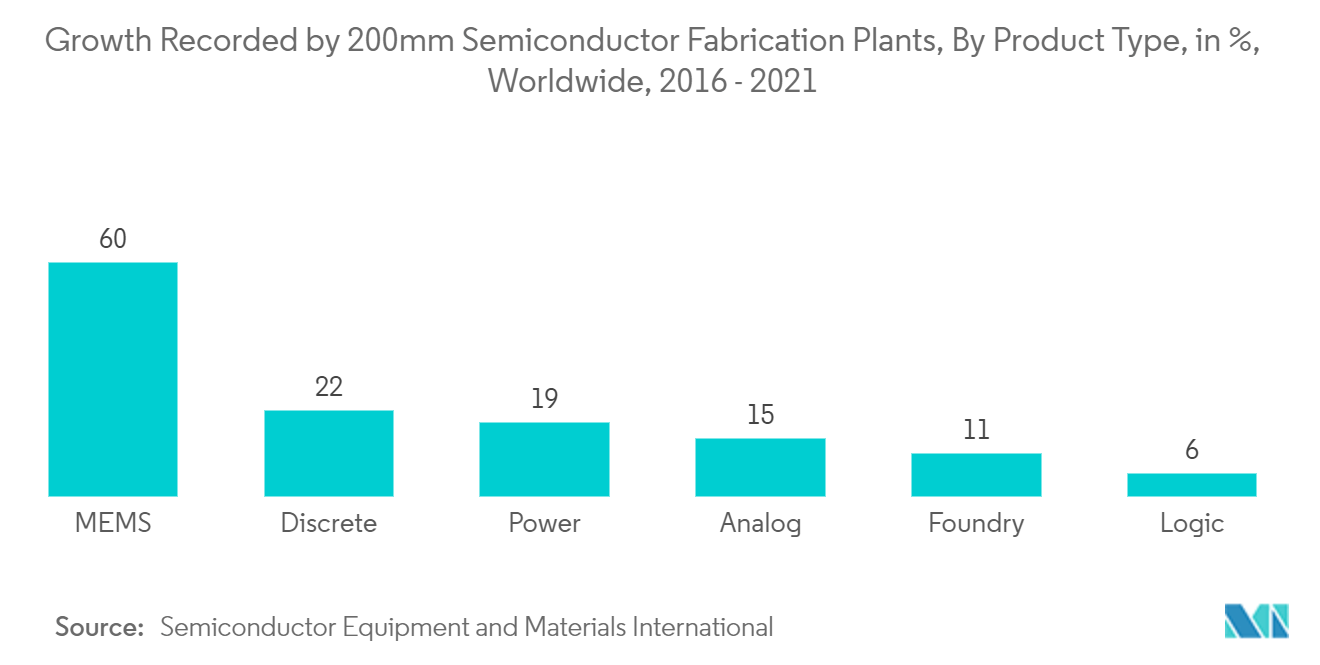
Power Electronics is Expected to Significant Share
- The growing need for power-efficient products is one of the major factors driving the demand for the epitaxial wafer for power electronics products across all the end-user industries. Therefore, the market vendors are targeting a wide range of industries to mitigate risk and expand their customer base.
- The IGBT and MOSFET markets may continue to increase, but a part of the market is expected to go to SiC, especially when discussing modules for EV/ HEV. Moreover, the demand for power MOSFET is supported by its growing use in replacing insulated-gate, bipolar transistors, and thyristors. Additionally, the significant advantage of using power MOSFET in reinforcing the power efficiency of devices at low voltages further drives the demand for the global power MOSFET market.
- The increasing usage of power electronics in consumer devices also fuels the demand. The growing penetration of smartphones and smart devices, increasing the adoption of IoT devices, and increasing industrial usage are also developing markets for power electronics. The high demand for power electronics devices has also resulted in a shortage of 200 mm wafers in 2018 and 2019. The customer demand is falling because major customers still have vast equipment inventory. The long-term growth in the power electronics market is also driving 300 mm wafer-based production. More than seven global power electronics vendors have announced an investment in new fabrication capabilities to be in production from 2021.
- Imec and Qromis have collaborated for the developed enhancement-mode, p-GaN discrete, and IC power devices on 200 mm QST substrates, with epitaxy layers grown in Aixtron's G5+ C 200 mm MOVCD platform. Both companies have been working on device fabrication, developing GaN power devices, indiscreet and monolithically-integrated ICs forms, and 200 mm QST substrates in an advanced CMOS silicon pilot line. Imec and Qromis have collaborated with Germany-based GaN MOCVD equipment manufacturer, Aixtron on GaN-on-QST epitaxy development. Many industrial experts claim that the number of integrated circuits (IC) semiconductor fabrication plants processing 300 mm wafers worldwide are expected to grow from 15 in 2002 to 138 by 2023.
Understand The Key Trends Shaping This Market
Download Sample
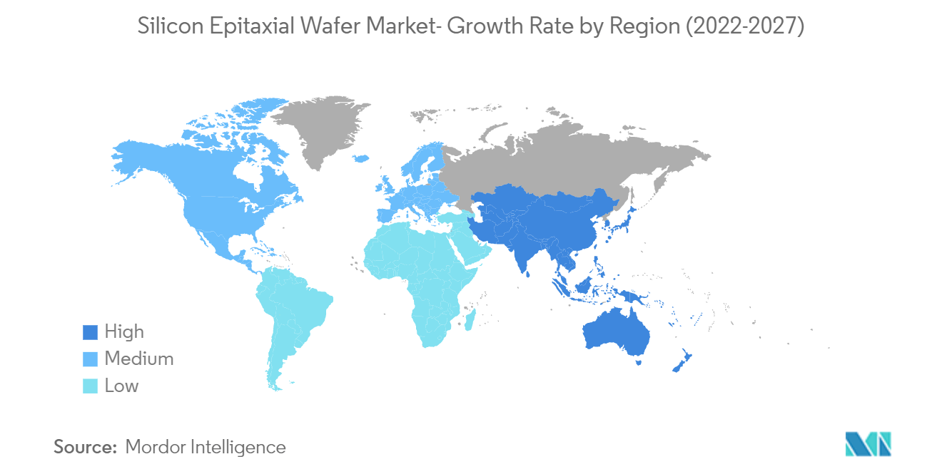
Asia Pacific is Expected to Hold Major Share
- The semiconductor wafer market is expected to ramp up 200 mm manufacturing between 2021-2022. The demand for 300 mm wafers is expected to grow by 2025; the market studied may also witness advancement and innovation. Due to their dominance in semiconductor manufacturing, Asia-Pacific is also dominating the market looked. The high market price of the SiC substrate and the growing LED demand forced many Asian manufacturers to GaN wafers. However, in 2019-2020, many Chinese LED manufacturers overproduced GaN wafers. The Metalorganic Chemical Vapour Deposition (MOCVD) market is also witnessing a significant overcapacity for GaN LED production compared to what is produced.
- The semiconductor industry of China has been showing an upward trend for the past ten years. According to China's Ministry of Industry and Information Technology, semiconductor sales by Chinese manufacturers reached USD 97.3 billion in 2018, which is around 20% of the global semiconductor revenue for the year. The country aims to produce 40% of the semiconductors it uses by 2020 and 70% by 2025.
- The Chinese government's Made in China 2025 national strategic plan has also been a significant factor in the publications' rise. The central aim of the plan is the growth of the semiconductor industry. Further, China's National Intellectual Property Administration (CNIP) 2021 budget anticipates 2 million filings per year till 2023, which is expected to drive the growth of the studied market.
- Moreover, TSMC cited its interest and finalized its plan to build an advanced 5-nanometer wafer plant in Arizona. The company's board of directors had also approved investing USD 3.5 billion in a wholly-owned foundry in Arizona. It also stated to spend a total of USD 12 billion from 2021 to 2029 to build a 12-inch wafer plant to produce chips using the advanced 5nm process.
Get Analysis on Important Geographic Markets
Download Sample
