Market Size of Semiconductor CVD Equipment Industry
| Study Period | 2019 - 2029 |
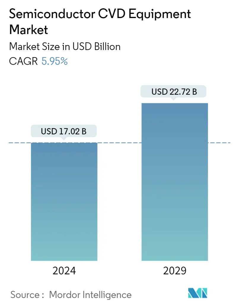
| Market Size (2024) | USD 17.02 Billion |
| Market Size (2029) | USD 22.72 Billion |
| CAGR (2024 - 2029) | 5.95 % |
| Fastest Growing Market | Asia Pacific |
| Largest Market | Asia Pacific |
Major Players
*Disclaimer: Major Players sorted in no particular order |
Need a report that reflects how COVID-19 has impacted this market and its growth?
Semiconductor CVD Market Analysis
The Semiconductor CVD Equipment Market size is estimated at USD 17.02 billion in 2024, and is expected to reach USD 22.72 billion by 2029, growing at a CAGR of 5.95% during the forecast period (2024-2029).
Increasing demand for microelectronics-based consumer products, resulting in the faster growth of the semiconductor, LED, and storage device industry and strict regulations on the use of Cr6 for electroplating are primarily driving the growth of the CVD equipment market.
- The Chemical Vapor Deposition (CVD) process is often used in manufacturing semiconductors and producing thin films. In recent years, CVD synthesis has reached new heights with the precise manufacturing of both inorganic thin films of 2D materials and high-purity polymeric thin films that may be conformally deposited on various substrates.
- Precursor gases (typically diluted in carrier gases) are supplied into the reaction chamber at around ambient temperatures in semiconductor chemical vapor deposition equipment. They react or break down when they pass across or come into touch with a heated substrate, generating a solid phase that is deposited on the substrate. The temperature of the substrate is important because it can influence the reactions that occur.
- CVD is widely used in microfabrication techniques to deposit materials in various morphologies, including polycrystalline, monocrystalline, amorphous, and epitaxial. Silicon (dioxide, carbide, nitride, oxynitride), carbon (fiber, nanofibers, nanotubes, diamond, and graphene), fluorocarbons, filaments, tungsten, titanium nitride, and a variety of high-k dielectrics are among these materials.
- Governments and business stakeholders are watching developments in the microelectronics industry closely because these technologies have the potential to disrupt and propel the Internet of Things market. Due to the increased adoption of virtual reality and augmented reality gadgets, R&D for microelectronics may also increase in response to the looming bandwidth constraint.
- They are making semiconductors. CVD setup can be complex and comes with huge costs. The foundries and Outsources Semiconductor Assembly and Test (OSAT) companies are likely to face increased pressure on capital expenditures as they continue to expand production to address the rising chip demand.
- The COVID -19 outbreak affected the overall semiconductor and chip fabrication market from the demand and supply sides. The nationwide lockdowns and closure of semiconductor plants have further fueled the supply shortage trend. However, these effects are likely to be short-term and temporarily affect the demand for CVD technologies. Moreover, government precautions globally to support automotive and industrial sectors could help revive foundry industry growth.
