
Technology, Media and Telecom
5th MayPricing Strategy for Semiconductor Components
3 Min Read
Next Generation Non-Volatile Memory Market is Segmented by Technology Type (MRAM, STT-MRAM, FRAM, and More), Wafer Size (200 Mm, 300 Mm, and 450 Mm and Above), Interface (DDR4/DDR5, PCIe/NVMe, and More), Application (Data-Center and Cloud, and More), End-User Industry (Consumer Electronics, IT and Telecom, BFSI, and More), and Geography (North America, South America, Europe, Asia-Pacific, and Middle East and Africa).
Market Overview
| Study Period | 2020 - 2031 |
|---|---|
| Market Size (2026) | USD 7.71 Billion |
| Market Size (2031) | USD 17.94 Billion |
| Growth Rate (2026 - 2031) | 18.41 % CAGR |
| Fastest Growing Market | South America |
| Largest Market | Asia Pacific |
| Market Concentration | High |
Major Players *Disclaimer: Major Players sorted in no particular order. Image © Mordor Intelligence. Reuse requires attribution under CC BY 4.0. |
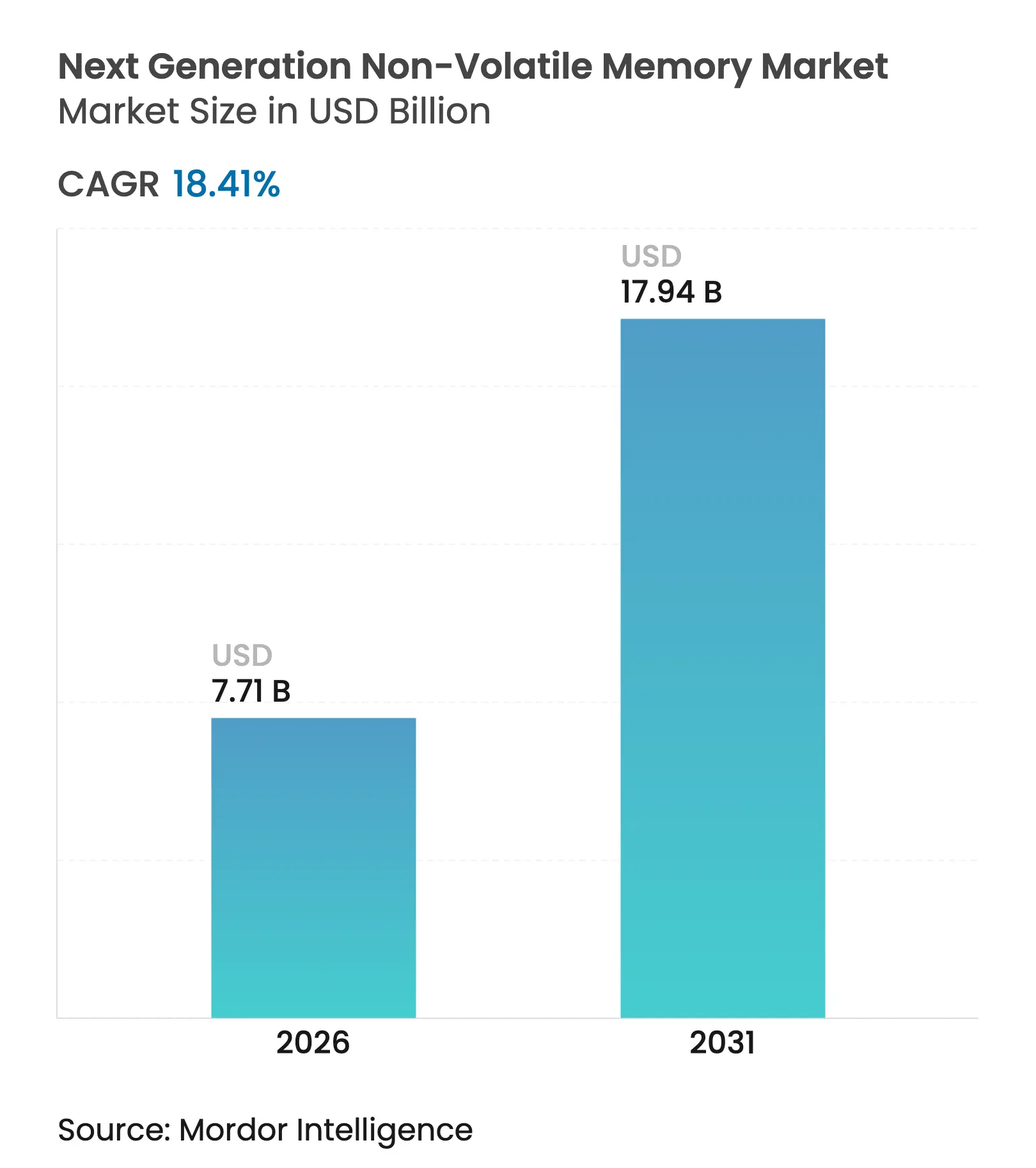
The Next-generation non-volatile memory market size is expected to grow from USD 6.51 billion in 2025 to USD 7.71 billion in 2026 and is forecast to reach USD 17.94 billion by 2031 at 18.41% CAGR over 2026-2031. This growth comes as data-intensive applications outpace the bandwidth and energy limits of conventional DRAM-plus-flash hierarchies, prompting systems designers to adopt persistent, high-speed alternatives. Large language model inference, the roll-out of zoned-storage architectures in hyperscale data centers, and stringent automotive reliability requirements are fuelling demand. Concurrently, semiconductor makers are leveraging advanced back-end processes such as magnetic tunnel junction deposition to boost bit density while trimming standby power. Strategic investments by foundries and integrated device manufacturers are easing supply-chain constraints and widening the adoption funnel for next-generation parts.
Key Report Takeaways
Note: Market size and forecast figures in this report are generated using Mordor Intelligence's proprietary estimation framework, updated with the latest available data and insights as of 2026.
Drivers Impact Analysis
| Driver | (~) % Impact on CAGR Forecast | Geographic Relevance | Impact Timeline | |||
|---|---|---|---|---|---|---|
Exploding AI/ML workload requirements in data-center
accelerators
Exploding AI/ML workload requirements in data-center
accelerators
| +5.2% | Global, with a concentration in North America and Asia-Pacific | Short term (≤ 2 years) |
(~) % Impact on CAGR Forecast
:
+5.2%
|
Geographic Relevance
:
Global, with a concentration in North America and Asia-Pacific
|
Impact Timeline
:
Short term (≤ 2 years)
|
Ubiquitous in-memory computation push from hyperscalers
Ubiquitous in-memory computation push from hyperscalers
| +4.3% | North America, Europe, Asia-Pacific | Medium term (2-4 years) | |||
Surge in automotive ADAS and domain-controller memory
bandwidth
Surge in automotive ADAS and domain-controller memory
bandwidth
| +3.8% | Global, with emphasis on Europe, North America, and Asia-Pacific | Medium term (2-4 years) | |||
Massive edge-IoT deployments needing ultra-low-power
persistent SRAM replacement
Massive edge-IoT deployments needing ultra-low-power
persistent SRAM replacement
| +3.1% | Global | Long term (≥ 4 years) | |||
Mainstream driver: Demand for high-speed, low-latency
storage (commercial)
Mainstream driver: Demand for high-speed, low-latency
storage (commercial)
| +2.5% | Global | Short term (≤ 2 years) | |||
Mainstream driver: Growing adoption of 5G and cloud gaming
(commercial)
Mainstream driver: Growing adoption of 5G and cloud gaming
(commercial)
| +1.9% | Asia-Pacific, North America, Europe | Medium term (2-4 years) | |||
| Source: Mordor Intelligence | ||||||
Exploding AI/ML workload requirements in data-center accelerators
High-bandwidth memory sales are multiplying as large foundation models drive parallel compute demand. Persistent, low-latency technologies allow GPUs and custom ASICs to cache multimodal parameters in situ, cutting energy associated with host-device transfers. SK Hynix is scaling new DRAM-compatible stacks to address AI throughput and has committed KRW 103 trillion to related capacity.[1]SK Hynix, “Record Quarterly Revenue Driven by AI Memory,” datacenterdynamics.com The ability to store models locally without refresh paves the way for turnkey inference nodes with materially lower total cost of ownership.
Ubiquitous in-memory computation push from hyperscalers
Cloud operators are trialling compute-in-memory arrays that execute multiply-accumulate operations inside non-volatile bit-cells, trimming data movement by up to 70%. Breakthroughs presented at IEDM 2024 demonstrated phase-change and resistive elements delivering analog matrix math for transformer workloads. As these arrays mature, the Next-generation non-volatile memory market gains a durable pull from AI inference at scale.
Surge in automotive ADAS and domain-controller memory bandwidth
Modern vehicles stream sensor data at 25 GB per hour, forcing domain controllers to couple high-bandwidth access with automotive-grade endurance. Embedded phase-change memory microcontrollers from STMicroelectronics retain data across -40 °C to 150 °C cycles, satisfying ISO 26262 safety profiles. Automakers now specify persistent memory for over-the-air firmware and event-data recorders, expanding the Next-generation non-volatile memory market footprint.
Massive edge-IoT deployments needing ultra-low-power persistent SRAM replacement
Battery-operated sensors often idle for long periods yet must preserve configuration data. FusionHD memories cut active power by 70% relative to standard flash while offering event logging and battery-health telemetry. For billions of edge nodes, such gains translate into multi-year operational life, reinforcing long-term demand.
Restraints Impact Analysis
| Restraint | (~) % Impact on CAGR Forecast | Geographic Relevance | Impact Timeline | |||
|---|---|---|---|---|---|---|
Integration yield loss at sub-10 nm BEOL layers
Integration yield loss at sub-10 nm BEOL layers
| -2.8% | Global, with higher impact in regions with advanced fabs | Medium term (2-4 years) |
(~) % Impact on CAGR Forecast
:
-2.8%
|
Geographic Relevance
:
Global, with higher impact in regions with advanced fabs
|
Impact Timeline
:
Medium term (2-4 years)
|
Capital-intensive EUV tooling scarcity
Capital-intensive EUV tooling scarcity
| -2.3% | Global, with a concentration in Asia-Pacific, North America, and Europe | Short term (≤ 2 years) | |||
Mainstream restraint: High manufacturing cost (commercial)
Mainstream restraint: High manufacturing cost (commercial)
| -1.7% | Global | Medium term (2-4 years) | |||
Mainstream restraint: Lack of unified interface standards
(commercial)
Mainstream restraint: Lack of unified interface standards
(commercial)
| -1.5% | Global | Long term (≥ 4 years) | |||
| Source: Mordor Intelligence | ||||||
Integration yield loss at sub-10 nm BEOL layers
Complex stack materials—cobalt, tantalum alloys, and ferroelectric oxides—introduce new defect mechanisms at advanced nodes. Cambridge researchers note that junction resistance variability undermines wafer yields for embedded MRAM and ReRAM, inflating the cost of goods. Until process controls improve, manufacturers balance density gains against economic risk.
Capital-intensive EUV tooling scarcity
A single EUV scanner exceeds USD 150 million and ships in limited volumes. ASML anticipates supply tightness extending to 2025, slowing fab ramps for sub-7 nm memory designs. Delays in securing lithography slots constrain the Next-generation non-volatile memory market during near-term demand surges.
By Technology Type: Carbon-Nanotube NRAM Unlocks Universal Memory Potential
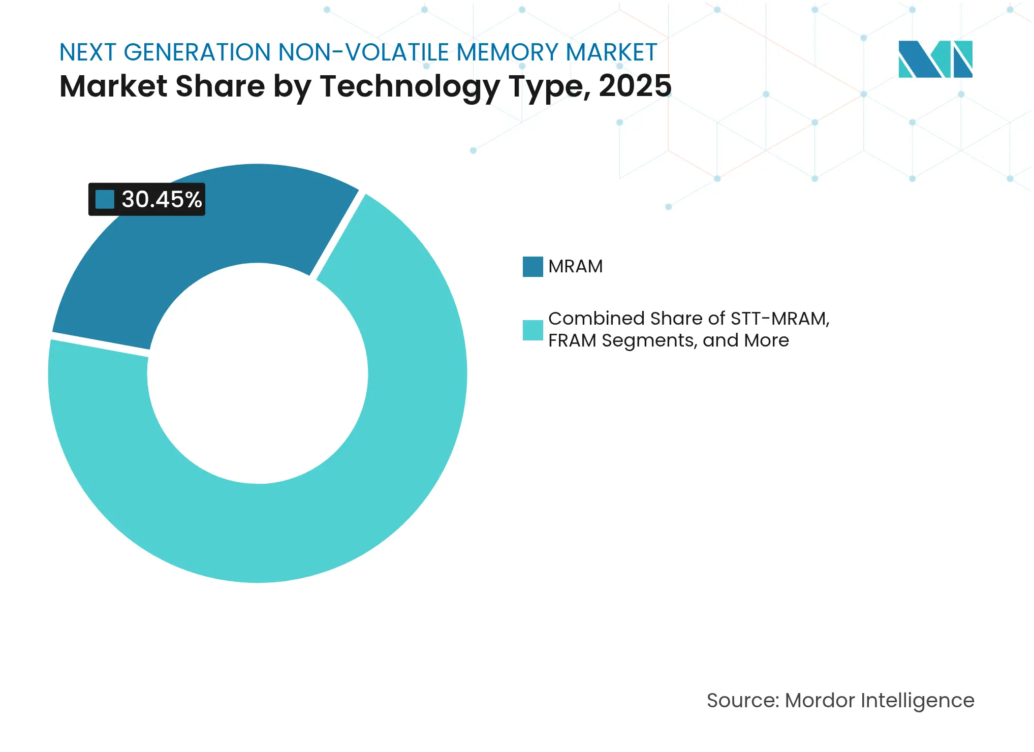
The segment’s revenue leadership rests with MRAM, which secured 30.45% of the Next-generation non-volatile memory market share in 2025 through its compatibility with standard CMOS back-ends. However, Nano-RAM is forecast to expand at 36.58% CAGR thanks to picosecond switching and endurance beyond 1 trillion cycles, placing it at the frontier of universal memory aspirations. Resultant performance positions NRAM to displace both DRAM and flash in high-performance embedded workloads, enlarging the Next-generation non-volatile memory market size for heterogeneous compute platforms.
Alternative technologies continue to broaden the landscape. ReRAM’s low-temperature deposition makes it an attractive choice for microcontroller co-integration, while updated phase-change alloys reduce resistance drift, reviving interest after the retirement of Optane products. Ferroelectric NAND research by Micron and Kioxia indicates potential path-finding routes for high-bit-density cell architectures. Each innovation targets a specific sweet spot, write energy, retention, or endurance, reinforcing the picture of a pluralistic market rather than a single-winner scenario.
Note: Segment shares of all individual segments available upon report purchase
By Wafer Size: 450 mm Economics Re-shape Scale Advantages
Next-generation non-volatile memory market size for 300 mm output remains dominant, yet 450 mm pilot lines are expected to post a 18.74% CAGR and shift cost curves downward by as much as 30% per die. Early adopters with the financial muscle to deploy mega-fabs aim to capture economies of scale and secure premium foundry slots for AI-class memory. These economics can reinforce barriers to entry, consolidating leadership positions within the Next-generation non-volatile memory market.
Conversely, 200 mm and legacy 300 mm nodes stay relevant for cost-sensitive industrial and automotive variants, where design rules above 40 nm suffice. Mature fabs already amortized allow specialty suppliers to deliver small-geometry ferroelectric or resistive parts without massive capex. This bifurcation ensures diversity in supply even as leading-edge geometries march to 3 nm.
By Interface: LPDDR5X Upshifts Mobile Bandwidth
DDR4/DDR5 currently capture the majority share within the Next-generation non-volatile memory market; nonetheless, LPDDR5X modules, operating at 0.5 V and 8,533 MT/s, are projected for a 27.25% CAGR. The tighter power envelope aligns with thin-and-light laptops, XR headsets, and AI accelerator edge boxes. Micron’s LPCAMM2 concept combines LPDDR5X with compression-attached packaging to yield 70% lower consumption and a 60% smaller footprint compared with SODIMM modules. Faster PCIe/NVMe protocols, as showcased by Solidigm’s 122 TB SSD, extend storage-class memory to exabyte-scale archives.
SPI/QSPI remain in wide use for embedded microcontrollers where simplicity and instant code-execute features outweigh bandwidth. Interface diversity, therefore, mirrors application diversity, underlining the segmented nature of the Next-generation non-volatile memory market.

Recognized by Experts. Trusted by Leaders.
A trusted intelligence partner to global decision-makers across 90+ countries.


By Application: Edge-IoT Devices Demand Power-Frugal Persistence
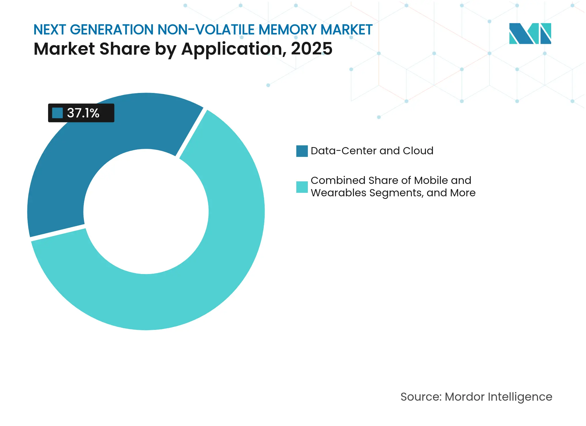
Edge-IoT endpoints are the fastest-growing application, forecast at 23.45% CAGR. Designers adopt persistent memories that wake instantly, log sensor data locally, and suspend again without loss, achieving multi-year battery life. In cloud settings, data-center and AI servers still hold 37.10% of overall revenue, relying on high-bandwidth stacks that keep large models resident near compute. This dual-track demand pushes suppliers to optimize both power per bit and gigabytes per second simultaneously, expanding the Next-generation non-volatile memory market on multiple fronts.
Mobile and wearables continue to spur interface evolution toward ever-lower voltages. Automotive infotainment and ADAS domain controllers need reliable instant-on storage that withstands thermal cycling, making multichip packages with combined volatile and non-volatile die an attractive solution.
Note: Segment shares of all individual segments available upon report purchase
By End-user Industry: Automotive Accelerates Memory Innovation
Consumer electronics remained the largest revenue contributor, taking 31.20% of the Next-generation non-volatile memory market share in 2025. Yet, automotive is the standout growth engine, racing forward at a 24.35% CAGR to 2031 as electrification and autonomous features proliferate. Vehicle electronics demand retention after sudden power loss and operate across wide temperature bands; embedded phase-change or FRAM elements satisfy these needs while enabling secure over-the-air updates.
Beyond mobility, the BFSI sector leverages persistent memory to accelerate fraud-detection analytics in real time, while aerospace programs procure radiation-hardened variants for on-orbit data handling. Such vertical diversification stabilizes demand and underpins the long-term addressable opportunity for the Next-generation non-volatile memory industry.
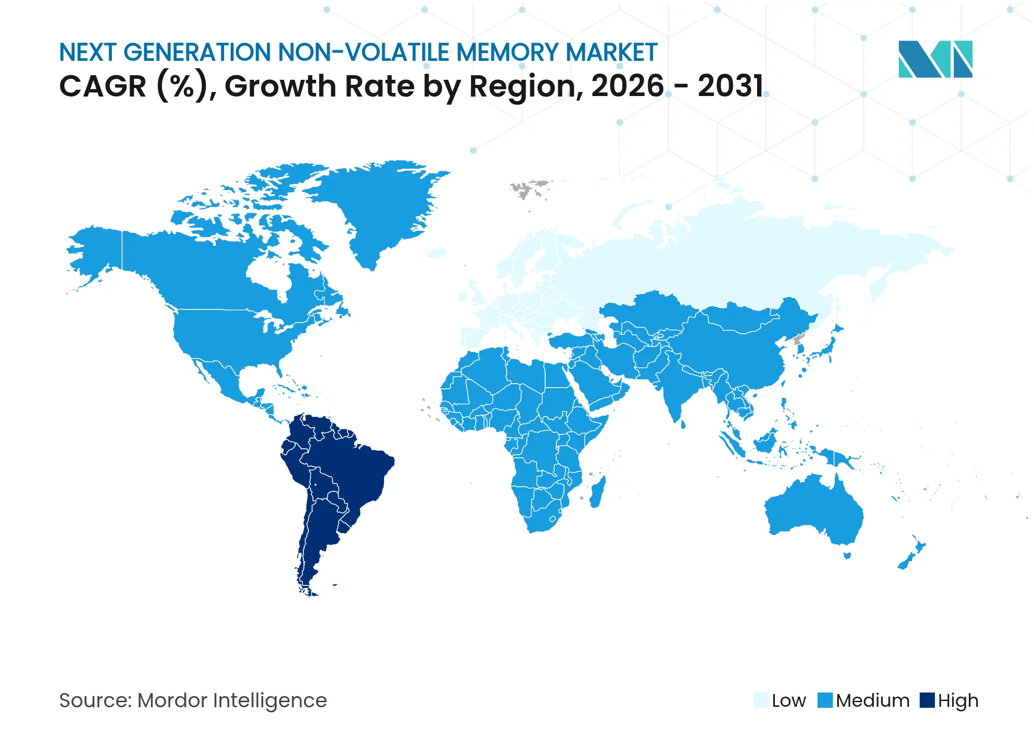
Asia-Pacific commanded 41.10% of the Next-generation non-volatile memory market in 2025, anchored by South Korean and Taiwanese giants with deep process know-how. Government incentives in Japan—such as a JPY 150 billion (USD 1.03 billion) subsidy to Kioxia and Western Digital—are widening 3D flash output using wafer-bond technology. Mainland Chinese fabs continue capacity build-outs under national self-reliance programs, while Singapore and Malaysia entice backend assembly with tax relief.
North America remains pivotal for advanced R&D, bolstered by the CHIPS and Science Act grants that fuel domestic pilot lines for embedded MRAM and ferroelectric logic. Flagship projects include Micron’s Idaho DRAM plant and Intel-built Ohio megafab clusters. Europe is on a catch-up trajectory; the EUR 10 billion (USD 11.60 billion) ESMC venture in Dresden couples TSMC’s 16/12 nm FinFET prowess with Bosch and Infineon’s automotive portfolios to localize supply.
South America is the fastest-growing cohort with a 19.72% CAGR projection. Brazil’s RUSD 650 million (USD 128 million) expansion by Zilia Technologies embodies public-private efforts to seed regional memory production. The Middle East and Africa, though smaller in absolute terms, register rising uptake in telecom and fintech verticals as sovereign digital-transformation agendas prioritize local data processing.
Market Concentration
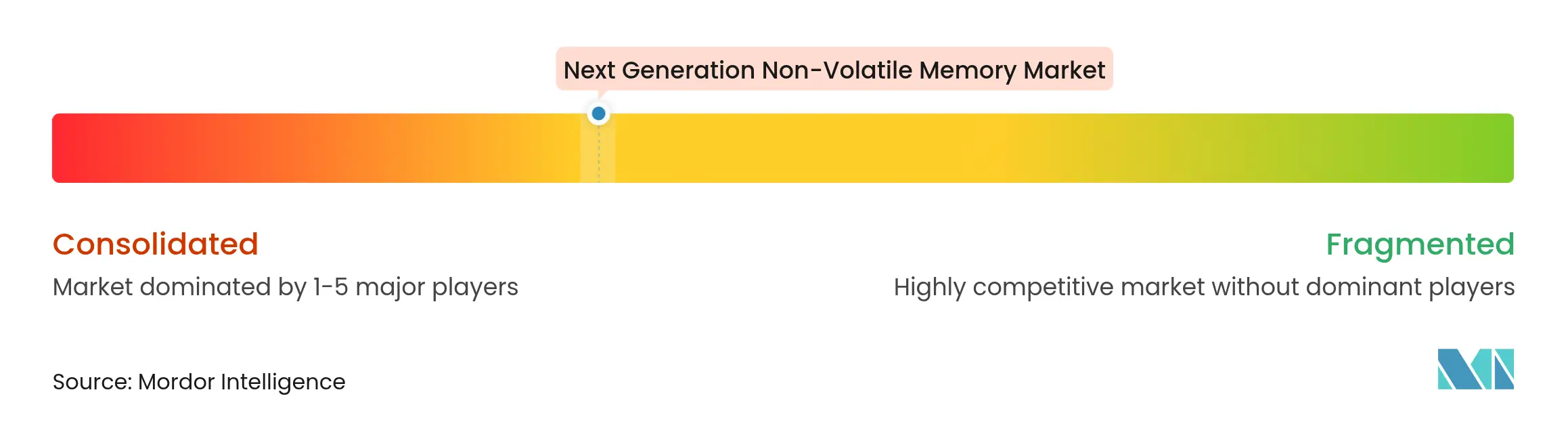
Industry leadership is moderately fragmented among vertically integrated majors—Samsung Electronics, SK Hynix, and Micron Technology—that control raw wafer fabs, advanced lithography, and proprietary controller IP. Collectively, the top trio accounts for well above two-thirds of high-performance bit shipments. Niche specialists are carving defensible positions: Everspin dominates discrete MRAM for industrial controllers; Weebit Nano recently taped out a 28 nm ReRAM module for embedded MCU clients; Nantero licenses CNT-based cells to defense contractors. The landscape is shifting from “one-size-fits-all” density races to application-specific differentiation—radiation hardening for satellites, power-fail protection for enterprise caches, or ultrafast write endurance for cache-coherent fabrics.
Strategic alliances multiply. Micron and Nanya relaunched their MeiYa Technology JV to share capex on next-gen DRAM lines.[4]Micron Technology Press Office, “Micron and Nanya Sign Agreement to Create Memory Technology Joint Venture,” Micron, April 21, 2008, micron.com Western Digital is spinning out its flash unit into a standalone Sandisk entity to sharpen focus on 3D-NAND advances. On the foundry side, SMART Modular partnered with Broadcom to co-design CXL-enabled E3.S modules for AI hosts, underscoring a migration toward composable memory fabrics.
As universal memory concepts mature, competition will pivot on ecosystem enablement: driver stacks, firmware features, and integration reference designs that simplify customer adoption. Suppliers that align road-maps with evolving interface standards—CXL, UCIe, or LPDDR6—are positioned to capture disproportionate value.

*Disclaimer: Major Players sorted in no particular order
1. INTRODUCTION
2. RESEARCH METHODOLOGY
3. EXECUTIVE SUMMARY
4. MARKET LANDSCAPE
5. MARKET SIZE AND GROWTH FORECASTS (VALUE)
6. COMPETITIVE LANDSCAPE
7. MARKET OPPORTUNITIES AND FUTURE OUTLOOK
Market Definitions and Key Coverage
Segmentation Overview
Detailed Research Methodology and Data Validation
Primary Research
Desk Research
Market-Sizing & Forecasting
Data Validation & Update Cycle
Why Mordor's Next Generation Non-Volatile Memory Baseline Commands Reliability
Benchmark comparison
| Market Size | Anonymized source | Primary gap driver | ||
|---|---|---|---|---|
USD 6.51 B (2025) | Mordor Intelligence | Anonymized source:Mordor Intelligence | Primary gap driver: | |
USD 8.20 B (2024) | Global Consultancy A | Includes traditional NAND and omits embedded-IP adjustment | ||
USD 6.82 B (2024) | Industry Association B | Blends volatile and non-volatile categories, fewer wafer tiers | ||
USD 8.35 B (2025) | Trade Journal C | Uses static ASPs and biennial forecast refresh |
Pricing Strategy for Semiconductor Components
3 Min Read
Accelerating Additive Manufacturing Adoption in India
3 Min Read
When decisions matter, industry leaders turn to our analysts. Let’s talk.