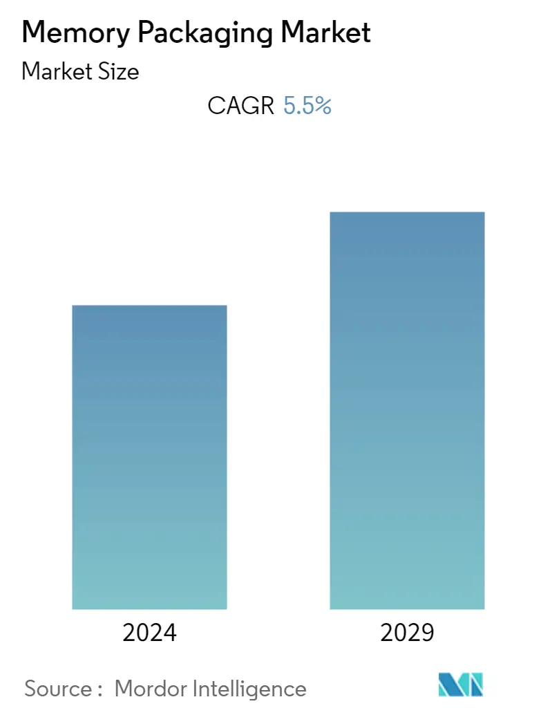
Market Size of Memory Packaging Industry
| Study Period | 2019 - 2029 |
| Base Year For Estimation | 2023 |
| CAGR | 5.50 % |
| Fastest Growing Market | Asia Pacific |
| Largest Market | Asia Pacific |
| Market Concentration | Medium |
Major Players
*Disclaimer: Major Players sorted in no particular order |
Need a report that reflects how COVID-19 has impacted this market and its growth?
Memory Packaging Market Analysis
The Memory Packaging Market was valued at USD 23.61 billion in 2020 and is expected to reach a value of USD 32.43 billion by 2026, at a CAGR of 5.5%, over the forecast period (2021 - 2026).
The recent COVID-19 outbreak is expected to create significant imbalances in the supply chain of the market studied, as Asia-Pacific, particularly China, is one of the major influencers of the market studied. Also, many of the local governments in the Asia-Pacific have invested in the semiconductor industry in a long run program, hence, expected to regain market growth. For instance, the Chinese government raised around USD 23 to 30 billion funds, to pay for the second phase of its National IC Investment Fund 2030. Owing to the uncertainty in the recovery time of the market from the pandemic, economic impacts on several parts of the world are further expected to provide significant challenges to the growth of the semiconductor market, directly affecting the availability of critical raw materials required for advanced memory packaging market globally.
- Memory devices employed a broad range of the packaging technology that include flip-chip, lead-frame, wire-bond, through-silicon via (TSV). With the decrease in dimensions and increase in the chip functionality, a higher number of the electrical connections have to be made to the external circuit.
- This has also led to development in packaging technologies. Flip-chip, TSV, and wafer-level chip-scale Packaging (WLCSP) are promising technologies to satisfy wider bandwidth, faster speed, and smaller/thinner package. Comprehensible program adjustments, low engineering costs, and easy changeovers are fueling the demand for the wire-bond memory packaging platform.
- Additionally, due to changes in the package design, the wire-bond memory packaging platform continues to be used as the most preferred interconnection platform because of its flexibility, reliability, and low-cost. Flip-chip began making inroads in the DRAM memory packaging in 2016 and was expected to grow due to its increased adoption in the DRAM PC/server, fueled by high bandwidth requirements.
- Spurred on by high bandwidth and memory chips' low latency demands for high-performance computing in numerous applications, through-silicon via (TSV), is being employed in high bandwidth memory devices.
