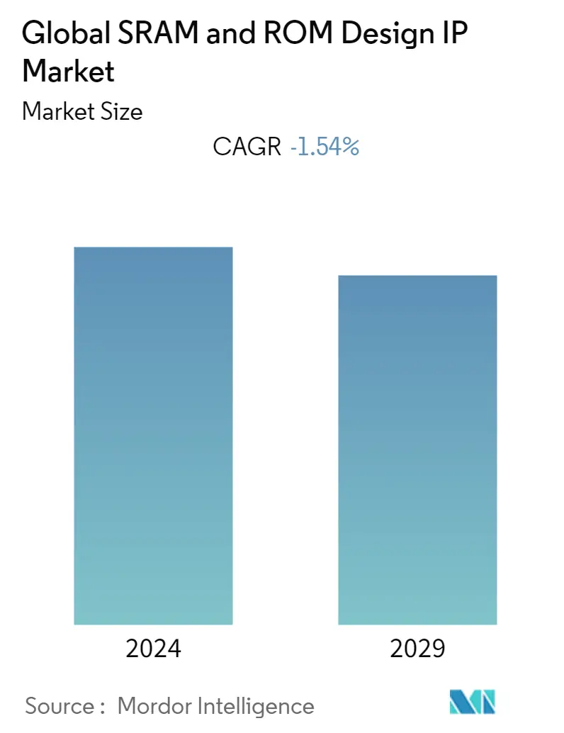
Market Size of Global SRAM and ROM Design IP Industry
| Study Period | 2019 - 2029 |
| Base Year For Estimation | 2023 |
| CAGR | -1.54 % |
| Fastest Growing Market | Asia Pacific |
| Largest Market | Asia Pacific |
| Market Concentration | Medium |
Major Players
*Disclaimer: Major Players sorted in no particular order |
Need a report that reflects how COVID-19 has impacted this market and its growth?
SRAM & ROM Design IP Market Analysis
The global SRAM Design IP market was valued at USD 627.26 million in 2020, and it is expected to reach USD 563.15 million by 2026, registering a CAGR of -1.54% and the global ROM Design IP market was valued at USD 190.54 million in 2020, and it is expected to reach USD 201.04 million by 2026, registering a CAGR of 0.87%, during the period of 2021-2026.
- Fast data volume growth and increasing preference for online content have encouraged storage producers to innovate continually. The demand for electronics components in the consumer electronics segment and microcontrollers, embedded systems, programable devices, and application-specific ICs in the industrial and scientific sector, automotive industry, continues to escalate the SRAM market.
- SRAM vendors are investing significantly to develop more efficient forms of SRAM technologies. For instance, OEM manufacturers are integrating more compact types of technologies in their product offerings and demanding small SRAM modules for their respective product offerings. For instance, as of December 2019, the Vision FPGA System on Module (SoM) by TinyVision.ai offered low-power computer vision and on-device machine learning in a compact package. The board is based upon Lattice iCE40UP5k FPGA, with 4Mb qSPI flash and 64Mb qSPI SRAM.
- ROM type of semiconductor memory technology is mainly used for storing programs and data that must survive even if a computer or processor is powered down. In recent years, the ROM memory is being increasingly replaced by flash memory. In general, maximum ROM memory capacity is lagging behind the flash memory (4-8 times), and in many of the original applications, ROM is replaced by flash memory, which experienced a significantly high growth in both capacity and market volume.
- However, the growing advancement in the EEPROM segment, especially in 2019, and emerging various new applications for microcontrollers, are some of the significant factors providing support to the ROM design IP market. Product innovations, in 2019, such as EEPROM memory chips, developed by semiconductor vendors for IoT and wireless applications in the medical, utility, and various other end-user industries, are expected to expand the scope of ROM design IP.
- For instance, in November 2019, STMicroelectronics launched its new generation of EEPROM memory chips for wireless and IoT applications. Microchip Technology's subsidiary Atmel's family of EEPROM chips are SPI compatible, offer max write cycles of 5ms and data retention of 100 years. These chips provide 4,096 bits of serial EEPROM and 8-byte page write. In July 2019, Europe-based NXP also launched a 4Mbit serial EEPROM that offers WLCSP like the M95M04-DR.
