Market Size of GaN Semiconductor Devices Industry
| Study Period | 2021 - 2029 |
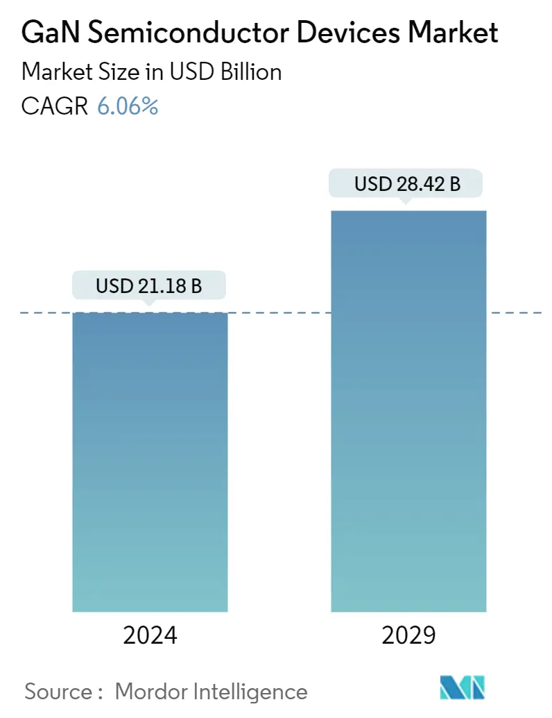
| Market Size (2024) | USD 21.18 Billion |
| Market Size (2029) | USD 28.42 Billion |
| CAGR (2024 - 2029) | 6.06 % |
| Fastest Growing Market | Asia Pacific |
| Largest Market | North America |
Major Players
*Disclaimer: Major Players sorted in no particular order |
Need a report that reflects how COVID-19 has impacted this market and its growth?
Gallium Nitride (GaN) Semiconductor Devices Market Analysis
The GaN Semiconductor Devices Market size is estimated at USD 21.18 billion in 2024, and is expected to reach USD 28.42 billion by 2029, growing at a CAGR of 6.06% during the forecast period (2024-2029).
GaN (gallium nitride) is creating an innovative shift throughout the power electronics sector. For decades, silicon-based Metal Oxide Semiconductor Field Effect Transistors (MOSFETs) have been an integral part of the everyday modern world that helps convert energy into power. GaN is replacing silicon as the backbone of power switching technology, as it can meet the growing needs with better power system performance, efficiency, and system cost.
- GaN is used to produce semiconductor power devices, RF components, and light-emitting diodes (LEDs). It has disrupted the technology for silicon semiconductors that are used in RF, power conversion, and analog applications. Increased semiconductor spending has a positive impact on the growth of the market under consideration.
- Also, the market for GaN semiconductor devices is being driven by the growing need for radio frequency in the semiconductor market, the growth of the consumer electronics industry, especially in LED-based lighting and displays, and the rise of electric vehicles, power delivery, and photovoltaic inverters.
- Further, GaN offers cost-effectiveness and the elimination of cooling requirements compared to silicon and gallium arsenide. In addition, the cost of production of a GaN device is much lower than the cost of production of a MOSFET device, as GaN devices are manufactured using standard silicon manufacturing procedures in the same factories where traditional silicon semiconductors are manufactured, and as GaN devices are much smaller for the same functional performance.
- The semiconductor device manufacturers are integrating an increasing number of passive components per circuit, leading to increased circuit design complexity and physical access limitations. This would require significant patterning that uses error-free masks to transfer the pattern onto wafers without any errors or defects. Therefore, OEMs' pressing need for an edge in device performance drives the market studied.
- Furthermore, with the growing development of wide bandgap (WBG) materials, market vendors are stimulated to manufacture small market products without compromising performance. GaN presents some unique challenges to the essential passive components used in power conversion and motor drive circuits to match the pace of innovations in the semiconductor process.
- The COVID-19 pandemic has led to enormous disruptions in supply chains across industries globally, due to which many businesses worldwide have halted or reduced operations to help combat the spread of the virus. The pandemic has impacted the studied market, leading to a drop in operation levels across the raw material production and supply chain for component production. This indicates a fall in sales among various countries and regions.
