Market Size of Embedded Die Packaging Industry
| Study Period | 2019 - 2029 |
| Base Year For Estimation | 2023 |
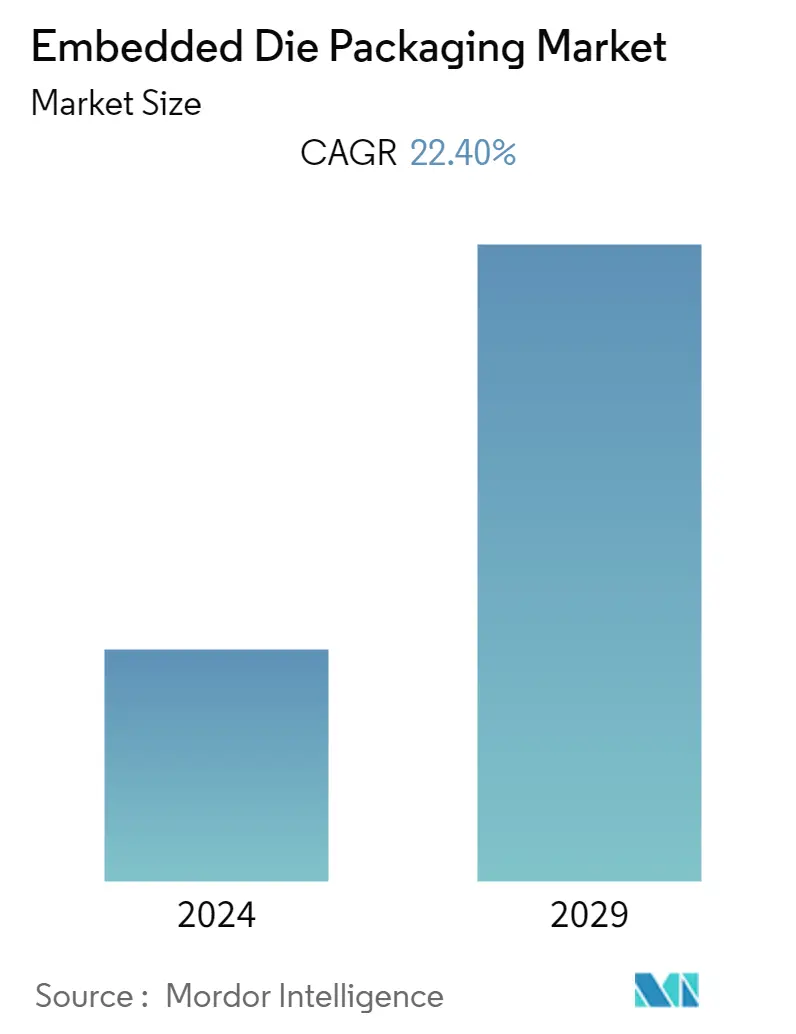
| CAGR | 22.40 % |
| Fastest Growing Market | Asia Pacific |
| Largest Market | North America |
| Market Concentration | Low |
Major Players
*Disclaimer: Major Players sorted in no particular order |
Need a report that reflects how COVID-19 has impacted this market and its growth?
Embedded Die Packaging Market Analysis
The embedded die packaging market was valued at USD 52.3 billion in 2020 and is expected to reach USD 175.27 billion by 2026 has been expected to grow at a CAGR of 22.4% during the forecast period (2021 - 2026). 3D packaging with embedded die solutions has become more attractive as an integration tool for next-generation devices which will become a key trend in future.
- Growing miniaturization of devices is driving the market as products are becoming increasingly smaller and embed more functionality. Micromachining and nanotechnology play an increasingly important role in the miniaturization of components ranging from biomedical applications to chemical microreactors and sensors. For instance, Bluetooth wifi modules requires minimal circuit board area on today's high-density mobile devices.
- Improved electrical & thermal performance is driving the market. For power management and mobile-wireless application the embedded technology has been evaluated to replace assembles fabrication by not only thinner thickness but due to superior thermal performance. The thermal performance of embedded die is better than PQFN with copper clip about 17%. Also a new and expandable advanced package for power devices is developed using embedded dies and redistribution layer (RDL) technology for electric car to improve the electric and thermal performance.
- Further, owing to its excellent electrical performance at high frequencies, the technology is also being perceived as a promising technology for emerging telecommunication applications. Various advantages that aid the deployment of the technology in telecommunication applications include increased functionality and efficiency of the electronic circuits, power and signal inductance, improved reliability, and higher signal density.
- Difficulty to test, inspect and rework, the embedded die technology challenges the market to grow. As features (lines and spaces) shrink to 2µm and below, it becomes more difficult to see defects. In addition, finding debris in via holes becomes a concern in some applications.
- Since the outbreak of COVID-19, the electronics industry has been hit severely, with a significant influence on its supply chain and production facilities. The production came to a stand still in China and Taiwan during February and March, which influenced various OEMs across the world.
