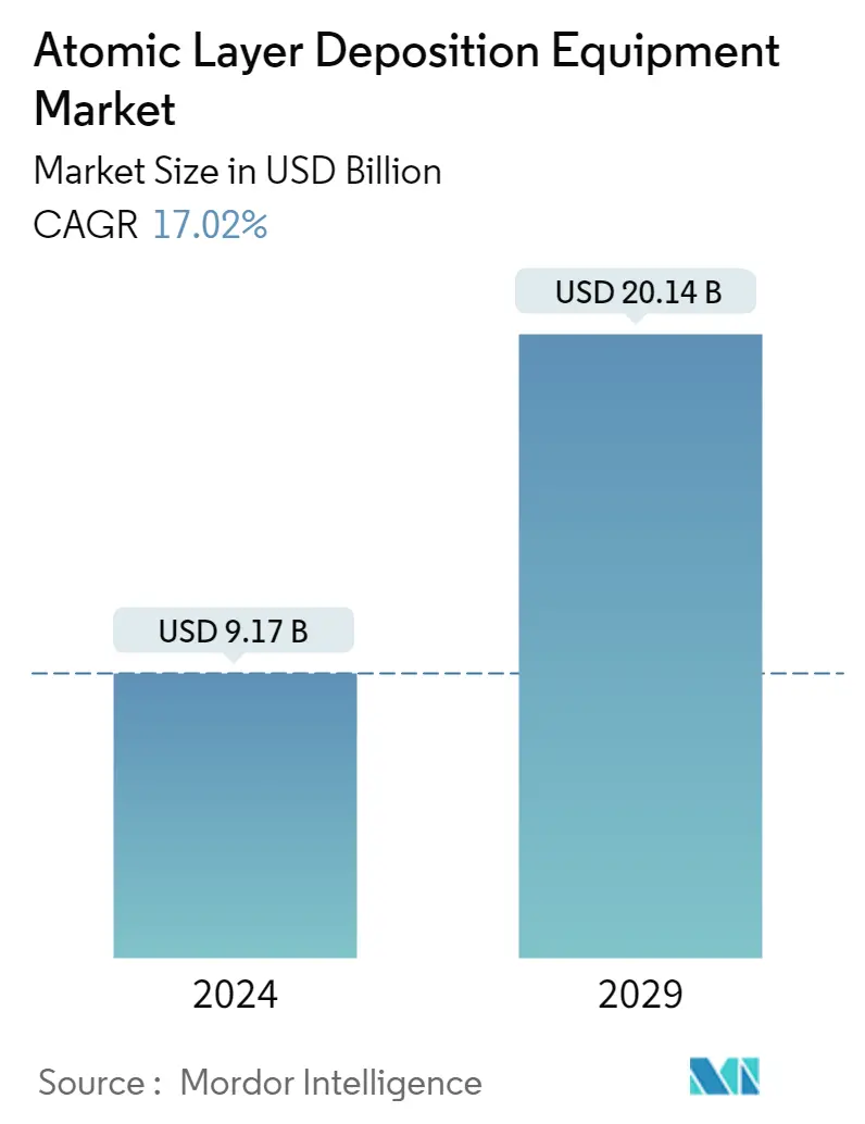
Market Size of Atomic Layer Deposition Equipment Industry
| Study Period | 2019 - 2029 |
| Market Size (2024) | USD 9.17 Billion |
| Market Size (2029) | USD 20.14 Billion |
| CAGR (2024 - 2029) | 17.02 % |
| Fastest Growing Market | Asia Pacific |
| Largest Market | North America |
Major Players
*Disclaimer: Major Players sorted in no particular order |
Need a report that reflects how COVID-19 has impacted this market and its growth?
Atomic Layer Deposition Equipment Market Analysis
The Atomic Layer Deposition Equipment Market size is estimated at USD 9.17 billion in 2024, and is expected to reach USD 20.14 billion by 2029, growing at a CAGR of 17.02% during the forecast period (2024-2029).
One of the key factors propelling the expansion of the worldwide atomic layer deposition market is the increasing adoption of electronics and semiconductor solutions across the globe.
- Using novel materials and designs for improved chip production drives demand for atomic layer deposition solutions. The trend toward miniaturization is being embraced by industries all around the world. As a result, there is currently a higher need for tiny electronics and machinery.
- According to Cisco, around 500 billion devices will be connected to the Internet by 2030. Each machine includes sensors that collect data, interact with the environment, and communicate over a network. These applications need miniaturized storage devices and ICs. The increasing amount of data generated from the growing number of connected devices has increased the demand for storage devices, thereby driving market growth.
- High-k dielectric films used in CMOS processors, memory devices, MEMS, and sensors are frequently produced using ALD in the semiconductor industry. For the creation of functional and protective coatings in fuel cells and other applications needing corrosion or wear resistance, ALD technologies are used. For the development of next-generation devices, they are also utilized to coat high aspect ratio structures like nanowires and nanotubes.
- Various deposition tools are employed to create semiconductors, including copper electrodes, high-K dielectric gate stacks, and copper barrier/seed layers. For instance, the domestic production of electronics in India increased from USD 29 billion in 2014-15 to USD 67 billion in 2020-21, according to data released by the country's national Investment Promotion & Facilitation Agency in March 2022, which is part of the Union Ministry of Commerce and Industry.
- Additionally, it is anticipated that greater robot use and manufacturing automation will promote the market for ALD technology by increasing semiconductor sales. Industrial automation is currently transforming the nature of practically all significant production industries. The adoption of Industry 4.0 standards and the increasing use of collaborative robotics, AR/VR, and AI for data analysis are anticipated to benefit the ALD market.
- Moreover, the ALD thin layer may be utilized in microelectronics to shield neighboring components in nanoscale transistors electrically. ALD is particularly adept at creating accurate, nanoscale coatings on intricate, 3D surfaces; such as the deep, narrow trenches etched into silicon wafers used to make modern computer processors. This has inspired researchers worldwide to create novel thin film ALD materials for upcoming semiconductor device generations.
- Over the projected period, a high investment required for research and development is anticipated to restrain the growth of the worldwide atomic layer deposition market. ALD is recognized to have significant limitations due to its slow approach.
- The atomic layer deposition industry's supply chain is still suffering due to the COVID-19 epidemic. The COVID-19 virus has a significant influence on many nations. Due to workforce shortages and disruptions in the raw material supply, the pandemic has hindered the production of atomic layer deposition materials. The development of ongoing projects was delayed due to these disruptions to international trade, which increased capital expenditure (CAPEX) and suspended the supply of atomic layer deposition.
