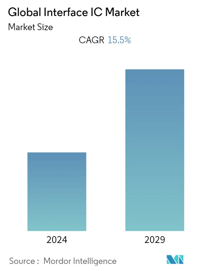
Market Size of Global Interface IC Industry
| Study Period | 2019 - 2029 |
| Base Year For Estimation | 2023 |
| CAGR | 15.50 % |
| Fastest Growing Market | Asia-Pacific |
| Largest Market | Europe |
| Market Concentration | Medium |
Major Players
*Disclaimer: Major Players sorted in no particular order |
Need a report that reflects how COVID-19 has impacted this market and its growth?
Interface IC Market Analysis
The Global Interface IC Market is expected to register a CAGR of 15.5% over the forecast period from 2022 to 2027. The outbreak of COVID-19 across the globe significantly disrupted the supply chain and production of the studied market during the initial phase of 2020. Due to labor shortages, many of the players in the semiconductor supply chain worldwide had to reduce or even suspend their operations, which affected the market growth.
The interface ICs are suitable for disposable medical devices and patches and sports and fitness equipment due to their small size and power-saving design. For instance, EnSilica, a fabless supplier of complex mixed-signal ASIC to OEMs, launched The ENS62020, an ultra-low-power healthcare sensor interface IC designed for monitoring vital signs in wearable healthcare and medical devices.
The interface integrated circuit (IC) can recognize the external power source and select one of two battery charge current levels based on the type. Signal communications between different electronic systems are controlled and managed by interface ICs. Depending on the communication protocol, these ICs determine how data is transmitted.
Semiconductor device manufacturers are integrating an increasing number of transistors per IC, leading to increased circuit design complexity and physical access limitations. It requires effective patterning that uses error-free masks to transfer the pattern onto wafers without any errors or defects. Therefore, the need for OEMs to have an edge in terms of device performance drives the market growth
Also, a diverse range of interface ICs enables dependable, efficient, and cost-effective connections while maintaining the highest signal isolation and protection standards.
However, the packaging and assembly houses have taken steps towards providing cost-effective solutions by offering flip-chip packaging options on a standard lead frame (FCSOL), quad flat pack no leads (QFN), and standard bis-maleimide triazine (BT) resin substrates. Whereas there may still be costs upfront in the wafer fabrication process, assembly houses are using proven technologies and innovative processes to provide customers with better solutions.
