Market Size of 3D TSV And 2.5D Industry
| Study Period | 2019 - 2029 |
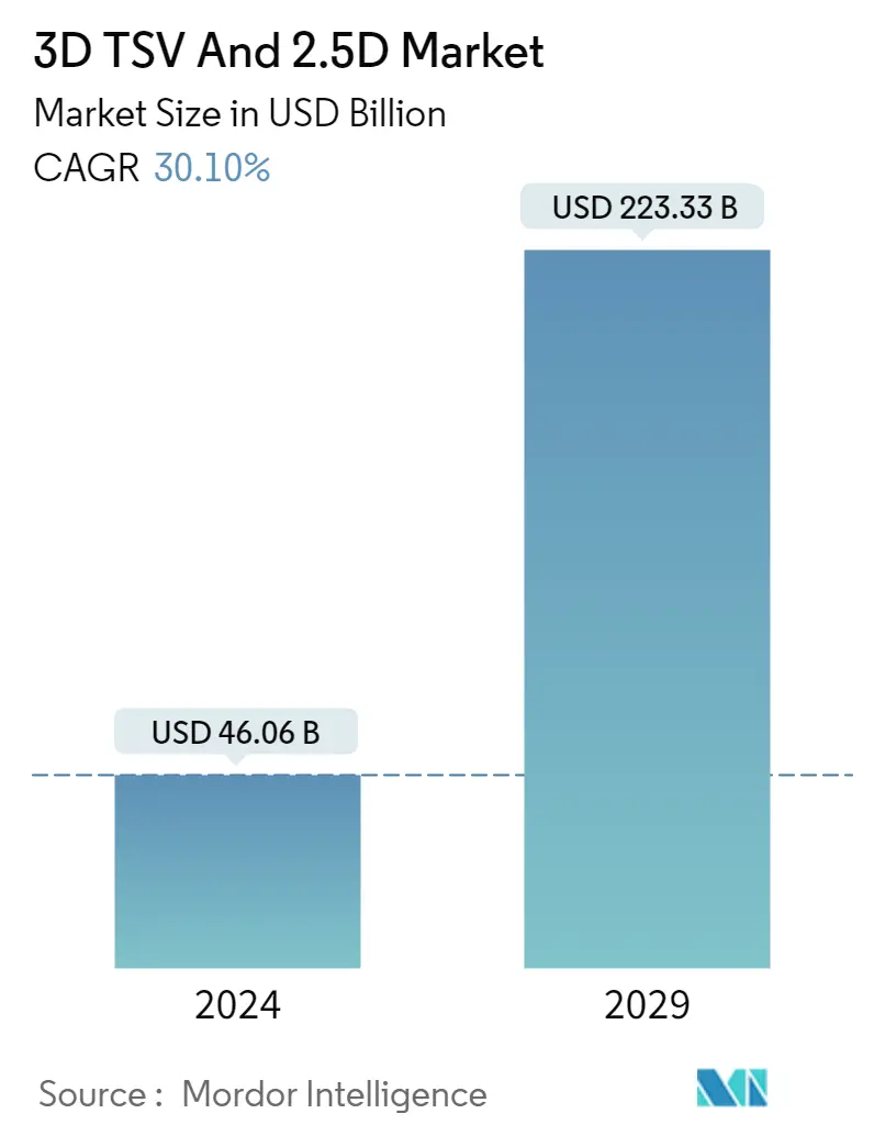
| Market Size (2024) | USD 46.06 Billion |
| Market Size (2029) | USD 223.33 Billion |
| CAGR (2024 - 2029) | 30.10 % |
| Fastest Growing Market | Asia Pacific |
| Largest Market | North America |
Major Players
*Disclaimer: Major Players sorted in no particular order |
Need a report that reflects how COVID-19 has impacted this market and its growth?
3D TSV And 2.5D Market Analysis
The 3D TSV And 2.5D Market size is estimated at USD 46.06 billion in 2024, and is expected to reach USD 223.33 billion by 2029, growing at a CAGR of 30.10% during the forecast period (2024-2029).
Packaging in the semiconductor industry has noticed a continuous transformation. As the semiconductor applications are growing, the slowdown in CMOS scaling and escalating prices have forced the industry to rely on the advancement in IC packaging. 3D stacking technologies are the solution that meets the required performance of applications like AI, ML, and data centers. Therefore, the growing requirement for high-performance computing applications mainly drives the TSV (Through Silicon Via) market over the forecast period.
- The 3D TSV packaging technology is also achieving traction. It reduces data transmission time between chips and the current wire bonding technology, resulting in significantly lower power consumption with faster speed. In October 2022, TSMC announced the launch of the creative 3DFabric Alliance, a considerable introduction to TSMC's Open Innovation Platform (OIP) to help customers overcome the surging hurdles of semiconductor and system-level design challenges. It will also help in gaining rapid integration of advancements for next-generation HPC and mobile technologies using TSMC's 3DFabric technologies.
- Increasing consumer demand for electronics has sparked the need for advanced semiconductor devices that enable various new capabilities. As the demands for semiconductor appliances intensify consistently, advanced packaging techniques deliver the form factor and processing power required for today's digitized world. For instance, according to the Semiconductor Industry Association, during August 2022, global semiconductor industry sales were USD 47.4 billion, a slight boost of 0.1% over the August 2021 total of USD 47.3 billion.
- In addition, according to the GSM Association, by 2025, the United States is expected to have the highest smartphone adoption globally (49% of connections). As per the United States IoT Association, it has the highest smart home device ratio per household and the most significant consumer tendency to own appliances across two or three use cases (energy, security, and appliances).
- Moreover, in September 2022, the Biden administration announced that it would invest USD 50 billion in building up the domestic semiconductor industry to counter dependency on China, as the US produces zero and consumes 25% of the world's leading-edge chips vital for its national security. President Joe Biden signed a USD 280 billion CHIPS bill in August 2022 to boost domestic high-tech manufacturing, part of his administration's push to increase US competitiveness over China. Such robust investments in the semiconductor sector would present lucrative opportunities for the growth of the studied market.
- The growth of MEMS and Sensors is attributed to the rapidly increasing demand for sensors and displays in various applications such as automotive, industrial automation, and many others. In August 2022, STMicroelectronics, a maker of MEMS and a significant player in the worldwide semiconductor industry, launched its third generation of MEMS sensors designed for consumer smart industries, mobile devices, healthcare, and retail sectors. The robust, chip-sized motion and environmental sensors power the user-friendly, context-aware features of today's smartphones, and wearables are made on MEMS technology. ST's most recent MEMS sensor generation drives technical boundaries regarding output accuracy and power consumption, elevating performance to a new level.
- Furthermore, the high costs associated with TSV device manufacturing restrict market growth. This includes not only the cost of devices but also the cost of accessories and consumables needed for their proper functioning. Moreover, the stringent guidelines and regulations governing TSV device manufacturing also add to the charges.
- Furthermore, the worldwide semiconductor shortage encouraged players to focus on expanding production capacity during a post-pandemic. For instance, the SMIC announced aggressive plans to double its production capacity by 2025 by constructing unique chip fabrication plants in different cities. Also, many Asian-Pacific local governments have funded the semiconductor industry in a long-term program, hence anticipated to regain market growth. For instance, the Chinese government introduced roughly USD 23-30 billion to pay for the second stage of its National IC Investment Fund 2030.
- Moreover, the ongoing conflict between Russia and Ukraine is expected to impact the electronics industry significantly. The conflict has already exacerbated the semiconductor supply chain issues and the chip shortage that have affected the industry for some time. The disruption may come in the form of volatile pricing for critical raw materials such as nickel, palladium, copper, titanium, aluminum, and iron ore, resulting in material shortages. This would obstruct the manufacturing of 3D Stacked Memory.
